On the PCB, designers often come across devices with metal casings. For example, reset button, USBinterface, network port, etc., but the shell of these devices, should be grounded? What place?
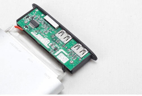
Grounding Design Without Metal Casing
No metal casing, PCB The components in the circuit board generally do not require grounding and cannot be grounded under normal conditions. For high-speed, high-power chips on a single board, designers can sometimes design a grounded heat sink. The heat sink is mounted on the PCB and connected to the ground plane of the board.
Grounded Design With Metal Casing
On PCB On the board, if you encounter a device with a metal case, you must ground it, and the case should be grounded in a large area. Otherwise, it will be difficult to meet the electromagnetic compatibility requirements of the device. The connector with metal case should be grounded. The casing or the bottom plate is tightly connected. If the connector is on the back plate, place all the connectors in a position close to a fixing screw. A grounding busbar is separately provided on the backing plate. The grounding busbar is connected to the metal casing of the connector. And connected to the grounded chassis through the fixing screws of the backboard, the grounding busbar and the other grounding wire or grounding surface of the backing plate should be separated by a certain distance. The grounding wire pin should be enough and should be arranged longitudinally, the grounding wire and the grounding Wire pin connections should be thick enough to avoid grounding bottlenecks. For high frequency signals, especially high frequency clock signals, the surrounding ground pins are surrounded.
For devices with metal casings, such as RS 232 interface, reset button, USB interface, network port, etc. Design engineers need to ground their enclosures, but improper grounding can cause problems. For these metal case devices, the grounding must be large, grounded at a single point.
Grounding Design of The Vacant Area on The Printed Board
In More Laminates wirings in the middle layer are large open areas, if not copper. In the PCB manufacturing process, since there is no copper foil on one side, when the pressure is pressed, the warpage is easily generated, and the entire circuit board is not flat. Moreover, the vacant area on the printed board should be coppered and grounded over a large area. Through holes should be enough, the ground connection should be thick enough. And remove the small area of the ground copper foil. Apply a large area of copper, pay attention to open a few slots to ease the foaming of copper foil. There is also: 1.The use of a cross-hair pad in a large area connected to the connector or IC pin facilitates soldering. 2. Ground the ground near the crystal oscillator. Be sure to set up the isolation strip. The crystal oscillator shell is connected to the ground. 3. The screw hole of the circuit board is preferably connected in series with a single point, not suspended. 4. Single-point grounding is used for digital ground and analog ground to prevent interference.



Hi, this is a comment.
To get started with moderating, editing, and deleting comments, please visit the Comments screen in the dashboard.
Commenter avatars come from Gravatar.