Rigid PCB Capability
| Item | Capability | Remarks | Illustrate | |
| Layers | 1-20 Layers | |||
| HDI | 1-2 Level | Mechanical blind burying or laser blind burying (hole can be filled by electroplating) | ||
| Material | FR4 | |||
| Surface Treatment | HASL Lead, HASL Lead Free, Immersion gold, OSP | |||
| Thickness | 0.6-2.5mm | Common thickness: 0.6/0.8/1.0/1.2/1.6/2.0/2.5, (3.0mm is available for batch produce) | 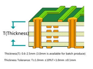 | |
| Thickness Tolerance | T≥1.0mm ±10% T<1.0mm ±0.1mm | |||
| Laser Hole Range | Used in blind hole plates, the tolerance of the laser hole is ±0.01mm | 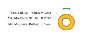 | ||
| Mechanical Drilling Range | 0.15-6.35mm | The minimum drilling hole is 0.15mm, and the maximum drilling tool is 6.35mm; holes >6.35mm need to be processed separately | ||
| Smallest Metal Slot | 0.45mm | The tolerance of slot hole diameter is ±0.1mm |  | |
| Smallest Non-metallic Tank | 0.8mm | The minimum gong knife is 0.8mm | 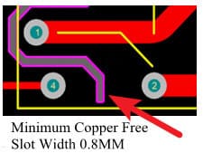 | |
| Drilling Thickness to Diameter Ratio | 1970-01-01 10:01:00 | The thickness of 0.2mm hole can be drilled to 2.0mm plate thickness | ||
| Hole Position Tolerance | ≤0.075mm | |||
| Aperture Tolerance | PTH | ±0.075mm | metal holes | |
| NPTH | ±0.05mm | non-metallic holes | ||
| Minimum Line Width/Line Distance of Inner Layer | 0.5oz | 3/3mil | 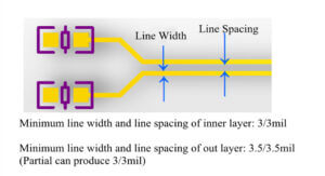 | |
| 1.0oz | 3.5/3.5mil | Local minimum 3/3mil can be produced | ||
| 2oz | 6/6mil | Local minimum 5/5mil can be produced | ||
| Minimum Line Width/Line Distance of Out Layer | 1.0oz | 3.5/3.5mil | Local minimum 3/3mil can be produced | |
| 2oz | 6/6mil | Local minimum 5/5mil can be produced | ||
| Smallest Via Hole Welding Ring | 3.5mil (single side) | Enlarging the protection area of the via welding ring to the hole increases, and the product is more reliable for long-term use | Image via | |
| Line tolerance | ±15% | |||
| BGA Pad Diameter | ≥0.2mm | BGA does not affect costs | ||
| Minimum BGA Pad Center Distance | 0.45mm | |||
| Plating Thickness (micro-inches) | Chemical nickel gold | Nickel thickness: 100-200 | ||
| Gold thickness: 1-3 | ||||
| Gold plating | Nickel thickness: 100-200 | |||
| Gold thickness: 1-10 | ||||
| Thickness of Porous Copper | Mechanical through hole | Lowest ≥20um | 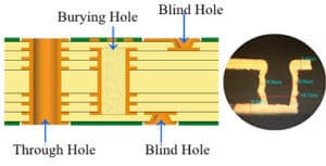 | |
| Blind hole | dimple≤15um | |||
| Buried hole | Lowest ≥20um | |||
| Cooper Weight | Inner Layer | 0.5-2oz | ||
| Out Layer | 1-2oz | |||
| Resistance Welding | Welding resistance window | ≥1.5mil | 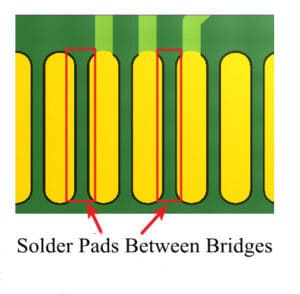 | |
| Welding Bridge | Green oil: 3.5mil Black oil, white oil: 5MIL Other inks: 4mil | |||
| Plug Hole | Plug hole diameter | 0.2mm ﹤hole diameter ≤ 0.45mm | ||
| Line etching | Line width / word height | ≥4mil/25mil | 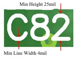 | |
| Silk Screen Characters | ||||
| Solder Mask Color | White, black, blue, green, red, yellow, etc., | |||
| Letter Color | Black, White | |||
| Max Size | 1 & 2 Layers | 500*600mm | ||
| Multi-layer | 400*500mm | |||
| Min Size | Width & Length | ≥10mm | ||
| Golden Finger Bevel | Angle | 20°, 30°, 45° | ||
| Angle tolerance | ±5° | |||
| Depth tolerance | ±0.15mm | |||
| Shape Tolerance | Regular shape | ±0.15mm | ||
| V-CUT | Angle | 20°, 30° | ||
| Maximum number of knives | ≤30 | |||
| Overall width | 55mm≤width≤480mm | |||
| Surplus thickness | 0.25mm≤Surplus thicknes≤0.5mm | |||
| Impedance | Impedance tolerance | ±10% | ||
| Test | Flying Test | Unlimited | ||
| Bench test | 14000 points | |||
| Panel & Multiple-block-joint | Zero gap make-up | The gap between the middle plate and plate is 0 | 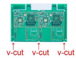 | |
| Gap make-up | The gap between the two pieces should be greater than 1.6 mm, otherwise it is difficult to cut the edge, which will affect the efficiency | 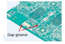 | ||
| Stamp hole mosaic | 0.5mm aperture and 0.3mm edge spacing of stamp holes, Conventional 5-7 holes in a group | 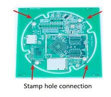 | ||
