Connection Design of Panelization And Auxiliary Edge
V-CUT Connection
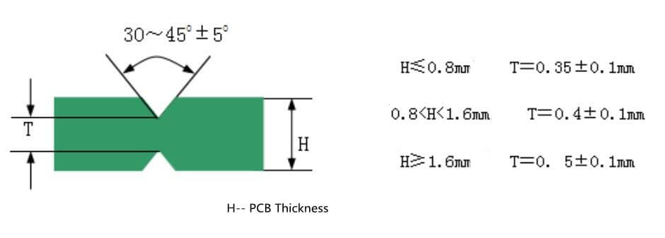
- V-CUT can be used when the PCB is connected in a straight line with flat edge and does not affect the device installation. V-CUT is straight through type and can’t turn in the middle.
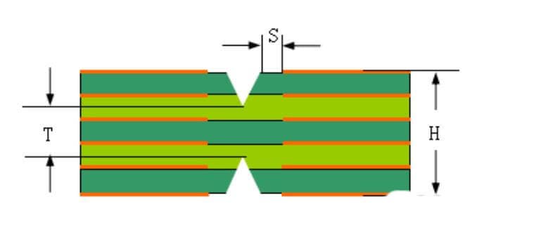
- The recommended thickness of PCB required by V-CUT design is ≤ 3.0 mm.
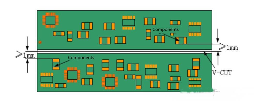
- For the PCB that needs to be divided automatically by the machine, the forbidden area of devices should be no less than 1 mm on both sides of the V-CUT line (top and bottom), so as to avoid damaging the devices during automatic dividing. (Figure 1)
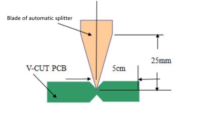
- At the same time, we need to consider the structure of the blade of the automatic splitter, as shown in Figure 2. It is not allowed to place the device whose height is higher than 25 mm within 5 mm away from the edge of the board. (Figure 2)
- When using V-CUT design, the above two items need to be considered comprehensively, and the one with harsh conditions shall prevail. Ensure that the components will not be damaged in the process of V-CUT, and the board can be divided freely. (Figure 3)
- At this time, the safety distance “s” from the edge of V-CUT to the edge of line (or pad) should be considered to prevent line damage or copper exposure. Generally, s ≥ 0.3mm is required. (Figure 4)
Stamp Hole Connection
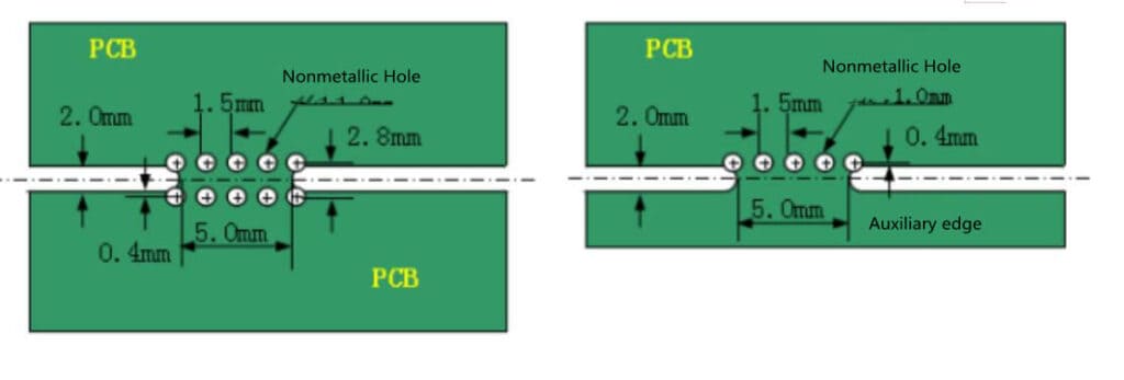
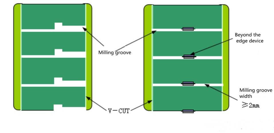
The recommended width of milling groove is 2mm. Milling groove is usually used when there is a certain distance between the unit plates, and it is generally used with V-CUT and stamp hole.
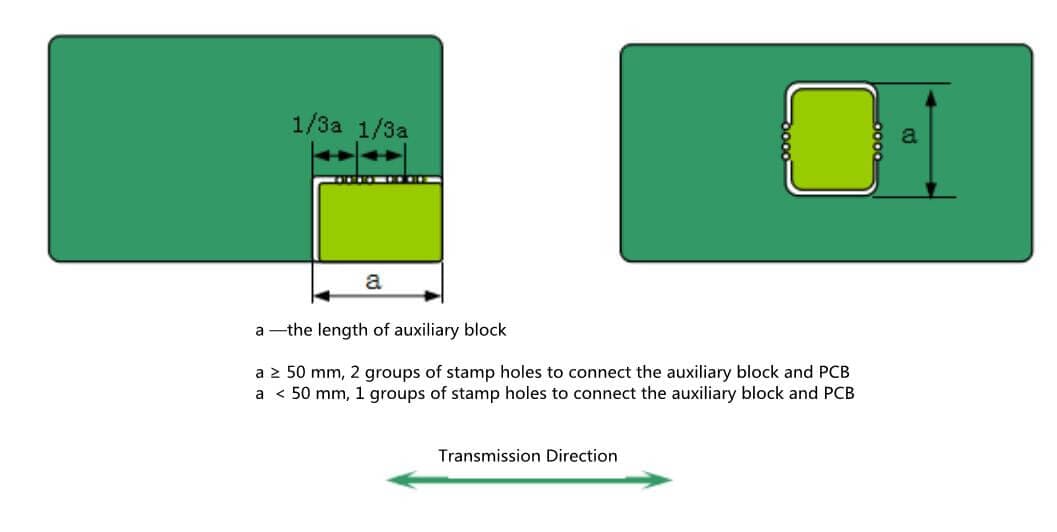
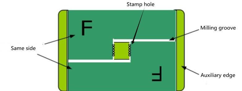
The design of stamp holes: the space between the holes is 1.5mm, and the recommended distance between the two groups of stamp holes is 50mm (Figure 5).
Panelization
There are three recommended Panelization ways: same direction, central symmetry and mirror symmetry.
When the size of PCB unit board is less than 80mm * 80mm, it is recommended to make Panel.
Designers need to consider the utilization rate of PCB board when designing PCB board, which is one of the important factors affecting the cost of PCB.
Note: For some irregular PCB (e.g. L-type PCB), using the appropriate splicing method can improve the utilization rate of the board and reduce the cost. (Show as Figure 6)
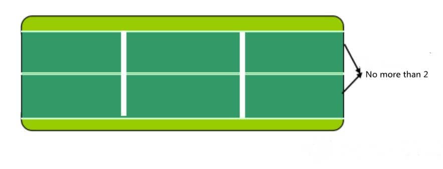
If the PCB needs reflow soldering and wave soldering, and the width of the unit board is more than 60.0 mm, the number of plates should not exceed 2 in the direction of vertical transmission edge. (Figure 7)
If the unit board is small, the number of plate splicing in the direction of vertical transmission side can exceed 3, but the total width perpendicular to the direction of single board transmission cannot exceed 150.0mm, and auxiliary tooling fixture shall be added in production to prevent deformation of single plate.
1. Same Direction Panelization
Regular cell board
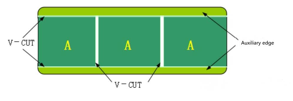
If PCB is in a straight line with flat edge, V-CUT is used for plate forming. And the plate assembly is allowed to be free of auxiliary edges. (Figure 8)
Irregular cell board
When the shape of PCB unit board is irregular or some components exceed the board edge, the method of milling groove and V-CUT can be used. (Figure 9)
2. Central symmetry Panelization
- Centrosymmetric plate making is suitable for two irregular PCBs. One side of the irregular shape is placed in the middle, so that the shape becomes regular after plate making.
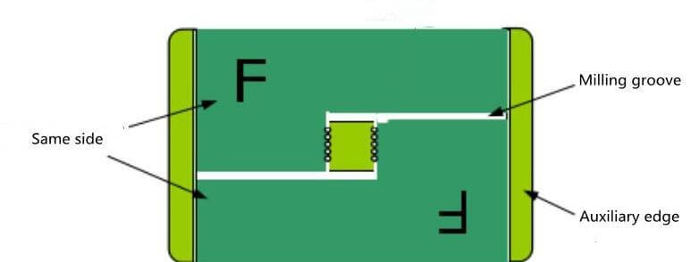
- The irregular shape PCB is symmetrical, and the milling groove must be opened in the middle to separate the two unit boards.
- If there is a large deformation of the plate, you can consider adding auxiliary blocks (connected with stamp holes) between the plates. (Figure 10)
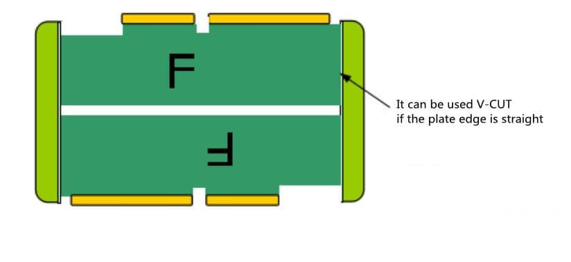
- For the card board with gold finger, it is necessary to make the gold finger face outward to facilitate gold plating. (Figure 11)
3. Mirror Symmetry Panelization
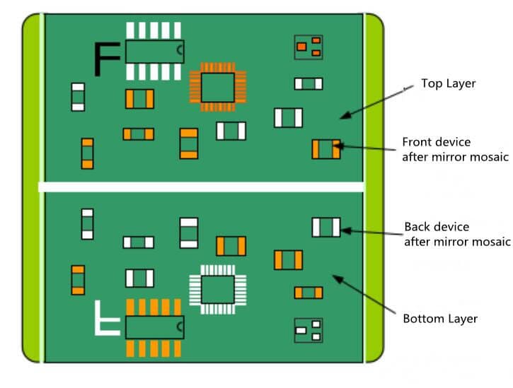
Conditions of use: when both sides of SMD meet the requirements of reflow soldering on the back side, mirror symmetry can be used.
Operation precautions: Mirror symmetrical plate making should meet the symmetrical distribution of positive and negative plates of PCB light drawing. Take the 4-layer board as an example: if the second layer is the negative film of power / ground, the symmetrical third layer must also be the negative film, otherwise the mirror symmetrical mosaic cannot be used. (Figure 12)
After using mirror symmetry, the auxiliary edge’s fiducial mark must meet the requirement of overlap after flipping. For specific location requirements, please refer to the reference point design of the plate below.
Connection Method of Auxiliary Edge and PCB
General Principles
- When the device layout can not meet the requirements of the width of the transmission edge (5mm forbidden area on the plate edge), the method of adding auxiliary edge should be adopted.
- When there are missing corners or irregular shapes on the edge of PCB board, and it can not meet the requirements of PCB shape, auxiliary blocks should be added to make up for the regular period, which is convenient for assembly. (Figure 13)
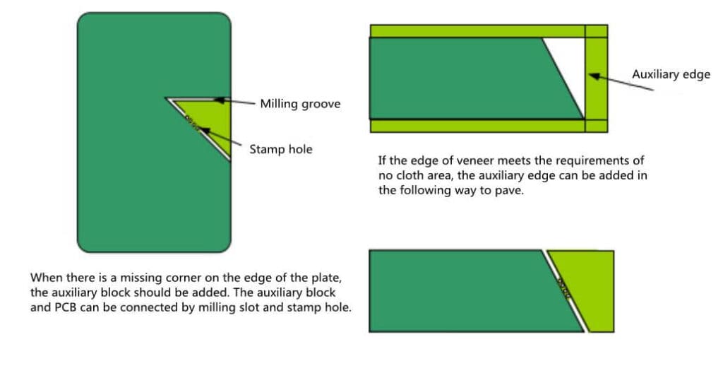
Plate edge and plate vacancy treatment
When there is a gap at the edge of the plate, or there is a gap greater than 35mm * 35mm in the plate, it is recommended to add an auxiliary block in the gap for SMT and wave soldering equipment processing. The connection between auxiliary block and PCB generally adopts milling groove + stamp hole. (Figure 14)
