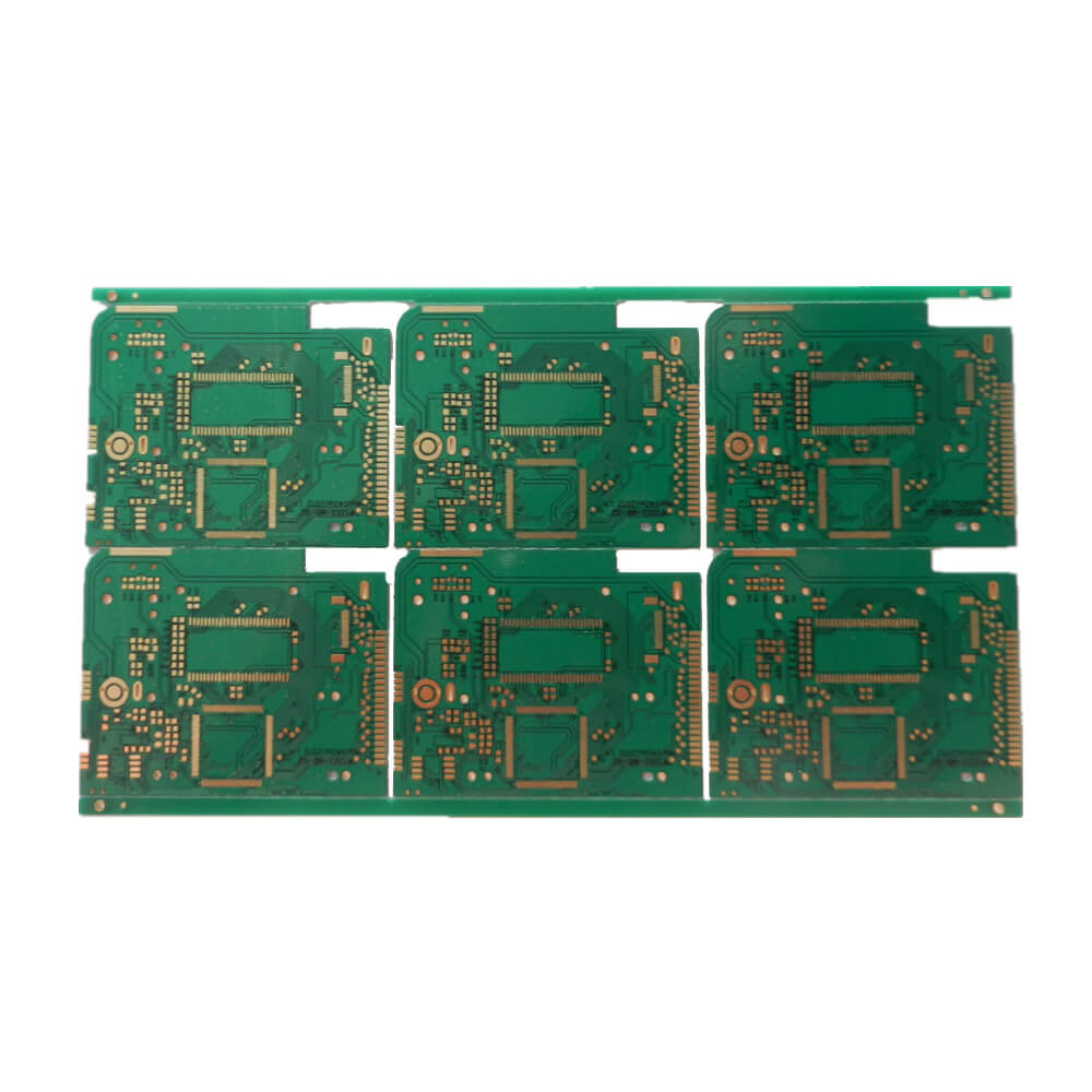
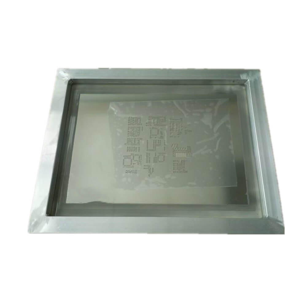
SMT Stencil
Shipping Way
Economy Express, Standard Express, Priority Express
Cost: Factory price
Leading Time:1 day
Production requirements: According to documents
Size: According the customer’s requirement
Custom: Yes
Introduction
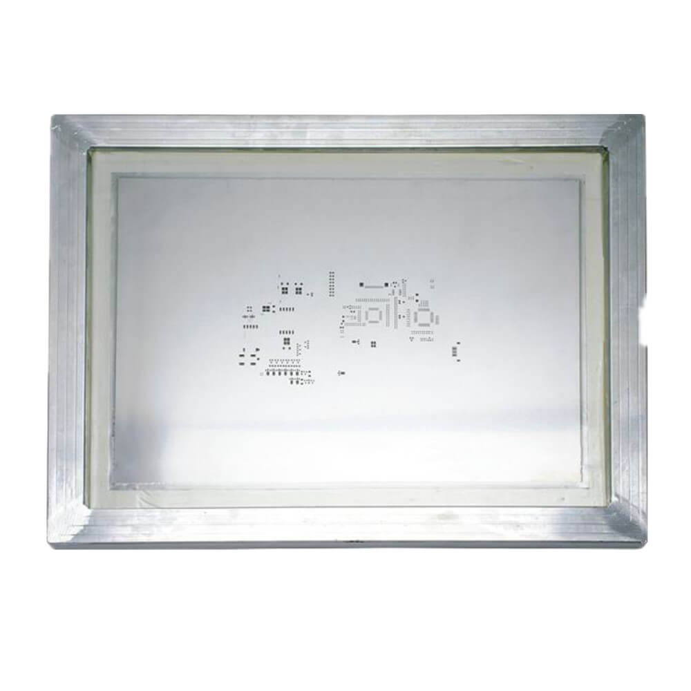
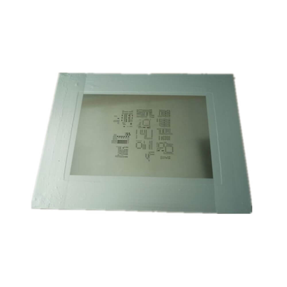
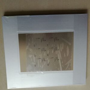
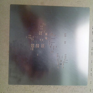
Stencil for PCB is also known as SMT stencil. It is a special mold for SMT. Its main function is to help the deposition of solder paste. The purpose is to transfer an accurate amount of solder paste to an accurate position on the empty PCB.
Category
According to the manufacturing process of SMT steel mesh, it can be divided into: laser stencil, Electro-polishing stencil, Electroforming stencil, step stencil, bonding stencil, nickel-plating stencil and etching stencil.
Laser stencil
Laser Stencil is currently the most commonly used template in the SMT steel mesh industry.
Features:
- Directly use data files for production, reducing production errors;
- The opening position of the SMT template is extremely accurate: the overall error is ≤±4μm;
- The opening of the SMT template has a geometric pattern, which is conducive to the printing and forming of the solder paste.
Two materials are required to make laser stencil, one is PCB, the other is data file.
Electro-polishing stencil (E.P. Stencil)
The Electro-polishing stencil is after laser cutting, through electrochemical methods to treat the steel sheet. Thus to improve the opening hole wall.
Features:
- The hole wall is smooth. It is especially suitable for ultra-fine pitch QFP/BGA/CSP.
- Reduce the number of wiping of the SMT template and greatly improve work efficiency.
Electroforming stencil (E.F. Stencil)
In order to comply with the requirements of short, small, light and thin electronic products, ultra-fine volume (such as 0201) and ultra-dense spacing (such as ūBGA, CSP) are widely used. As a result, the SMT steel mesh industry also proposes more printing templates. High requirements, Electroforming stencil came into being.
Step stencil
Due to the different requirements for the amount of solder paste when soldering various components on the same PCB, the thickness of some areas of the same SMT template is required to be different. It leads to the STEP-DOWN&STEP-UP process template.
Bonding stencil
The COB device has been fixed on the PCB, but the patch process of tin printing is still required. In this case bonding stencil is required. The bonding stencil is to add a small cover at the PCB bonding position corresponding to the template, in order to avoid the COB device and achieve the purpose of flat printing.
Nickel plated template (Ni.P. Stencil)
The nickel-plated template combines the advantages of the laser stencil and the Electroforming stencil.
Etching stencil
It is made of 301 type steel sheet imported from the United States. The etched steel mesh is suitable for PCB printing with corners and spacing greater than or equal to 0.4MM. It is suitable for copying and film use.
Production Process of Stencils
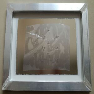
The production process of stencil includes: chemical etch, laser cutting and electroform.
Chemical etch Process flow
PCB data file→ film production→ exposure→ development→ etching→ steel cleaning →screening
Features: One-time molding, faster speed; low price.
Disadvantages:
- It is easy to form an hourglass shape (not enough etching) or the opening size becomes larger (over etching);
- Objective factors (experience, medicine, film) have a large influence, there are many production links, and the cumulative error is large.
- It is not suitable for fine pitch steel mesh production method ;
- The production process is polluted, which is not conducive to environmental protection.
Laser Cutting Technological Process
Film making PCB→ acquisition of coordinates→ data file→ data processing →laser cutting→ polishing→ screening
Features:
- High precision of data production, small influence of objective factors;
- Trapezoidal opening is good for demoulding;
- It can be used for precision cutting;
- Moderate price.
Disadvantages: cutting one by one, the production speed is slow
Electroform Process Flow:
Coating photosensitive film on the substrate→ exposure→ development→ electroforming nickel→ forming→ steel cleaning→ screening
Features: The hole wall is smooth, which is especially suitable for the ultra-fine pitch steel mesh production method.
Disadvantages: The process is difficult to control. It is not conducive to environmental protection. The production cycle is long and the price is too high.
Why Choose Us?
- Competitive Price
- Quality Warranty
- Excellent Service
- 24 Hours Fast Production
- 99.9% On-time Delivery
- Manufactured in China
Custom Service
Contact Us Now
Related Products
Production Process & Blog
How to Restore Deleted Isolated/hollowed-out Copper?
To restore deleted isolated copper or hollowed-out copper skin in...
Read MoreBest PCB Suppliers for Small-Batch Production
Looking for reliable PCB manufacturers specializing in low-volume orders? Here...
Read MoreDry Film & Application Processes
The company uses dry film in the production process, combined...
Read More
