The Schematic Design
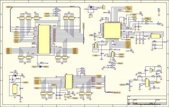
Schematic design is preparatory work. For a simple board, if you are with skilled process, you can skip it. But for beginners, you must follow the process. On one hand, you can develop good habits, on the other hand we can avoid mistake by this way for complex circuits. When drawing the schematic diagram, the hierarchy design should pay attention to the connection of each file as a whole, which is also of great significance for future work. Due to the difference of software, some software may appear to be connected but not connected (in terms of electrical performance). If you don’t use the relevant detection tools to detect, it will be too late to find out until the board is ready once there is wrong. Thus it shows the importance of the schematic design.
The Specific Process And Skills of Plate Making in Alutim Designer
1. Make physical frame
“Place > line” then draw the frame and select the box. Finally “design > board shape > define from selected objects”, finished. The main thing is to pay attention to accuracy, otherwise the installation problem will be a big trouble in the future. There is the best corner with arc, it’s not only avoid being scratched by sharp corners, but also reduce stress.2. Introduction of components and networks
Open the schematic and select “Design > Update PCB document” Common problems: the package form of components can’t be found, network problems of components, unused components or pins, which can be solved quickly accord the tips.3.Layout of components
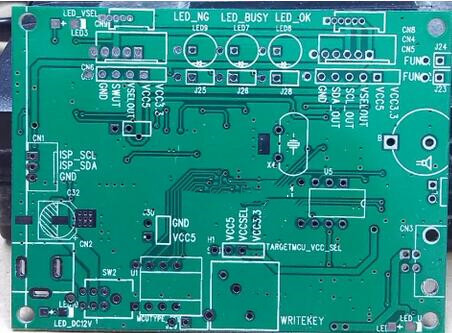
The layout and routing of components have great influence on the life, stability and electromagnetic compatibility of products, which should be paid special attention to. Generally speaking, there should be the following principles: (1) Placement order First place the fixed position components related to the structure, such as power socket, indicator light, switch, connector and so on. After these components are placed, lock them with the lock function of the software, so that they will not be moved by mistake. Then place special components and large components on the line, such as heating element, transformer, IC, etc. Finally, the small device is placed. (2) Pay attention to heat dissipation Special attention should be paid to heat dissipation in component layout. For high-power circuits, those heating elements such as power tubes and transformers should be placed as far away as possible, so as to facilitate heat dissipation. They should not be concentrated in one place, and high capacitance should not be too close, so as to avoid premature aging of electrolyte.4. Wiring
General Wiring Principle:- High frequency digital circuit should be thin and short
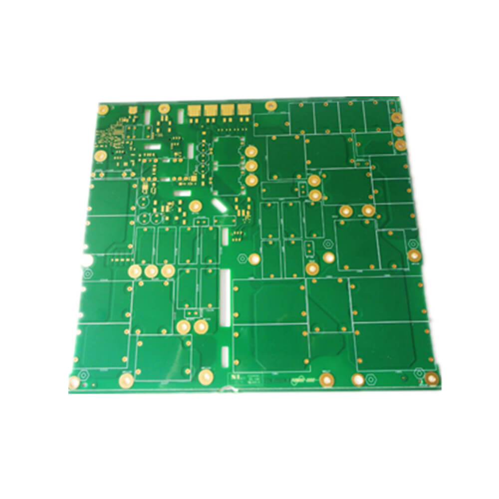
- Large current signal, high voltage signal and small signal should be isolated (isolation distance is related to withstand voltage. In many cases, in order to avoid creepage, slots are also made between high and low voltage on the printed circuit board.)
- When wiring the two panels, the wires on both sides should be perpendicular, skew or bent to avoid parallel to reduce parasitic coupling; As the input and output of the circuit, the printed wires should avoid the adjacent parallel as far as possible, so as to avoid feedback. It is better to add grounding wire between these wires.
- The routing corner should be 120 degrees as far as possible
- For the same address line or data line, the difference of routing length should not be too large, otherwise the short line should be compensated by artificial bending
- Routing should be on the welding surface as far as possible, especially for PCB with through hole technology
- Minimize the use of vias and jumpers
- The single panel pad must be large, the line connected to the pad must be thick, and tear drops can be released if they can. Generally, the quality of single panel manufacturers will not be very good, otherwise there will be problems with welding and re-work.
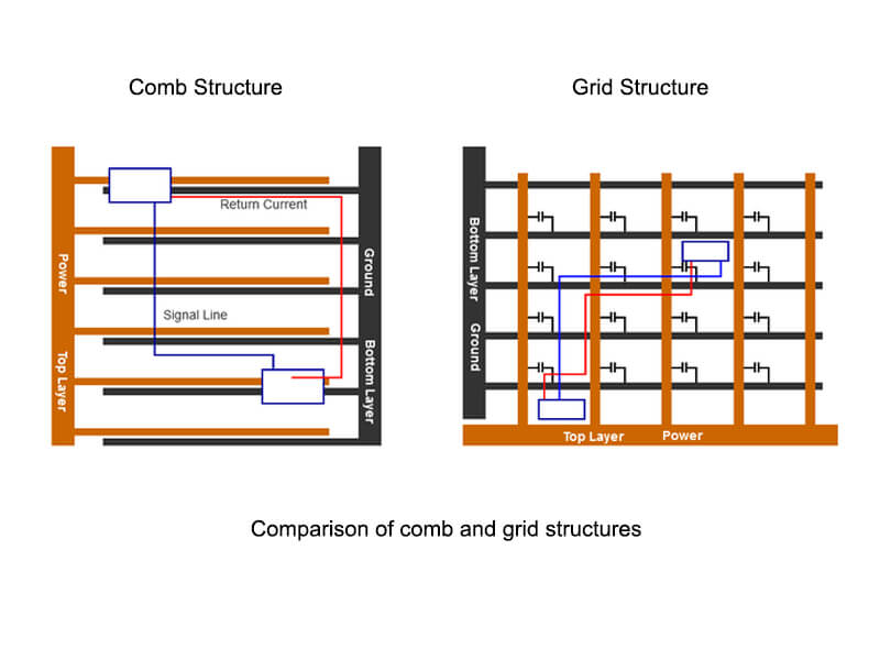
- In order to prevent bubbles and bending due to thermal stress during wave soldering, large area copper should be laid in grid shape. However, in special cases, the flow direction and size of GND should be considered. Instead of simply filling with copper foil, the wiring should be done.
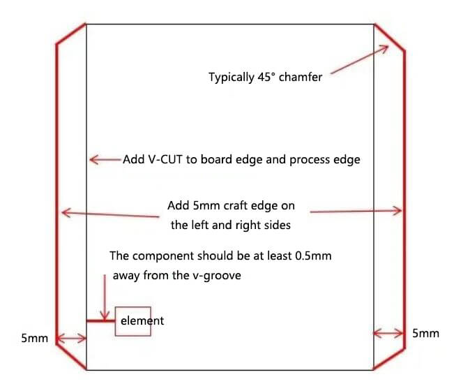
- The components and wiring should not be placed too close to the side. Generally, the single panel is mostly paper board, which is easy to break after being stressed. If the components are connected or placed at the edge, they will be affected.
- The convenience of production, debugging and maintenance must be considered.
- For serpentine wiring, because of different applications, its function is also different. It is used in some clock signals, such as pciclk and AGP CLK, in the main board of the computer. Its function has two points: 1. Impedance matching; 2. Filter inductor.

