General selection principle of grounding mode
For a given equipment or system, it is regarded as a high-frequency circuit when the length of the transmission line L > in at the highest frequency of interest (corresponding wavelength). On the contrary, it is regarded as a low-frequency circuit. According to the rule of thumb, for circuits below 1MHz, it is better to adopt single point grounding; for circuits above 10MHz, it is better to adopt multi-point grounding. For frequencies between the two, single point grounding can be used to avoid common impedance coupling as long as the length L of the longest transmission line is less than 1 / 20 in.
The general selection principles for grounding are as follows
(1) Low frequency circuit (< 1MHz): single point grounding is recommended;
(2) High frequency circuit (> 10MHz): multi-point grounding is recommended;
(3) High and low frequency hybrid circuit, hybrid grounding.
System Grounding Mode
Common mode interference, crosstalk and radiation interference are closely related to the grounding design of PCB. A good design can effectively control the impedance and area of the signal circuit, as well as the amplitude of the interference current.
For system grounding, the following considerations shall be taken into account at the early stage of PCB design to ensure the signal quality on PCB.
- Determine the possible interference sources in the circuit. It is generally high DI/ DT and high DV / DT circuits, such as clock, Bus Buffer / driver and high-power oscillator. Pay special attention to PCB layout, wiring and inspection.
- Identify sensitive circuits that are susceptible to interference in the circuit, such as low-level analog circuit, high-speed data and clock. Pay attention to isolation and protection during design.
- Ensure to minimize the low inductance and signal circuit. Therefore, the signal line should be as short as possible and the signal circuit area should be as small as possible. For high-speed circuits, multi-layer boards with ground plane should be used.
- Determine the divided and undivided part of the ground plane. For hybrid circuits, such as digital and analog division, the problem of signal crossing and signal loop will not appear or can be well solved, so division can be adopted. Otherwise, it is recommended to adopt the method of “partition but not division”. That is: strictly distinguish digital and analog areas during local and wiring to avoid common return path between digital signal and analog signal. But the strata are not separated. Avoid signal crossing to form a large signal circuit.
- The interface ground shall be well designed to keep the interface ground “clean”, so that the noise cannot be coupled into and out of the system, especially the signal connected by cable is easy to couple the noise into and out of the system. Pay attention to keep the I / O ground free from common mode interference, and the power ground of the interface part shall be plane as far as possible.
- Pay attention to the reasonable division of the circuit and control the common mode current between different modules. For pure digital circuits, pay attention to the division according to the high, medium and low working rate of the circuit and I / O. To reduce the common mode current between circuit modules.
- The grounding design on PCB shall comply with the general grounding scheme of equipment system. In particular, where the veneer, backplane and frame need to be overlapped, the PCB should be equipped with installation holes, tin spraying or conductive contact surfaces with other coatings required by the system.
Design of Double-sided PCB Grounding Structure
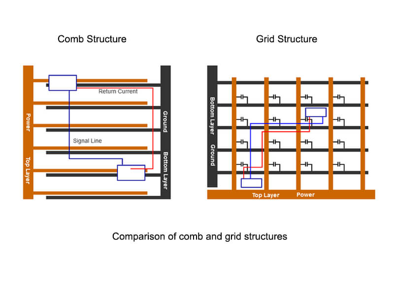
There are generally two types of double-layer board grounding, including “comb power supply, grounding structure” and “grid grounding structure”. Each type has its own suitable scene, but generally speaking, any circuit should not directly adopt comb grounding structure. It can be seen from the figure that the return flow of signal must be folded back to the root, and the loop area is large. However, as long as the heavier signals are protected, the empty places are covered with ground copper sheet after the wiring is completed, and multiple vias are used to connect the two layers of ground together, this defect can be made up. This structure is only suitable for low-speed circuits, where the direction of the signal on the PCB is relatively single and the routing density is low.
In the grid type ground structure, the power supply and ground are respectively led out from the top layer and bottom layer of the PCB in an orthogonal way, a decoupling capacitor is placed at the intersection of the power supply and ground, and both ends of the capacitor are connected to the power supply and ground respectively. Compared with comb type, the signal circuit of grid type ground structure is smaller. The grid ground structure is suitable for low-speed CMOS and ordinary TTL circuits, but it should be noted that sufficient ground protection should be added to the higher speed signals to minimize the loop area and the inductance of the return path.
Design of Single-sided PCB Grounding Structure
It is inappropriate to put forward specific requirements for grounding at the circuit level. For specific boards, we generally carry out necessary segmentation according to the device manual. For the connection between different types of ground on a single board, it is recommended to complete it through magnetic beads, or directly through a single point on the PCB. For the power supply directly connected to a single point without magnetic beads, it is recommended to place a 0.1uF (or 0.01uF) capacitor at the single point junction for filtering (one end is connected to the power supply and the other end is connected to the corresponding ground).
In the division of power supply and ground, we should pay attention to the way of cutting off EMI from primary to secondary through the reference plane, especially in the division of filters, common mode coils, magnetic beads and other devices.
The following is the ground division diagram of its isolation transformer provided by pulse company.
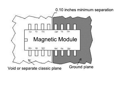
For the above figure, we notice that on the ground division of the isolation transformer
1) Location of division: primary and secondary connection
2) Width of dividing line: not less than 100mil.
The reason for the above segmentation processing is to achieve the isolation of the primary and secondary, and the interference at the control source is coupled to the secondary through the reference plane. From the following division diagram recommended by Intel, we can also find that the position of the division line is very important. In addition to achieving the function of isolation, we also need to consider the wiring of adjacent layers to avoid important signal lines crossing divided areas.
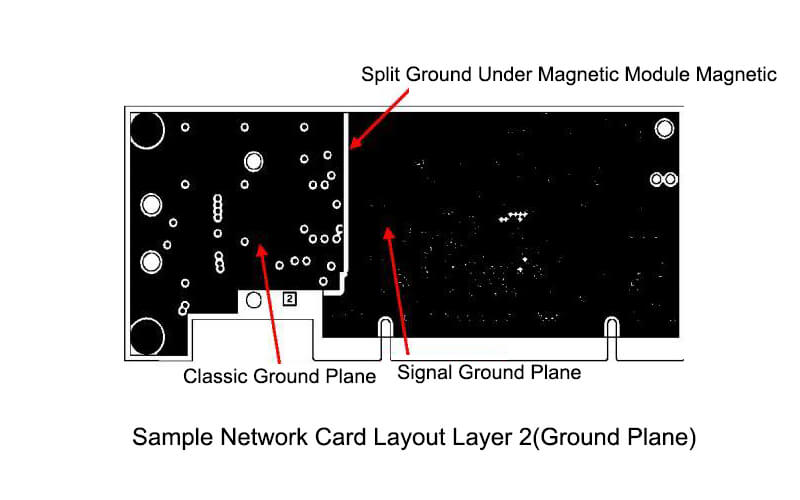
For most of the IC’s we use now, suppliers generally provide detailed PCB design requirements (including the division of power supply and ground). Hardware personnel should carefully analyze these requirements together with CAD engineers. Try to follow the requirements of the supplier when the actual situation is possible.
Multi-layer PCB Grounding Structure Design
When the frequency of the signal is low, the return of the signal is mainly along the path of the lowest resistance, that is, the geometric short-circuit path; When the signal reaches a certain frequency (F > 1kHz), the return current of the signal is concentrated along the lowest inductance path, and the return current mainly flows back below the printed line.
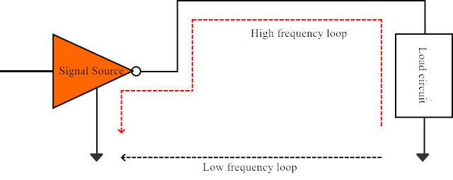
When the frequency is high, whether the signal is close to the power plane or the ground network plane, the return current of the signal always flows back along the close reference plane.


