General Requirements for Components Layout
- The THD componentswith polarity or direction shall be in the same direction in layout and arranged as orderly as possible. For SMD components, if the direction is consistent, it should be consistent in X and Y directions as far as possible, such as tantalum capacitance.
- If the componentneeds to be rubbed, it is necessary to leave at least 3mm space at the dispensing place.
- The SMD where the radiator is to be installed shall pay attention to the installation position of the radiator. Enough space shall be provided for the layout to ensure that it does not touch other components. Ensure that the minimum distance of 0.5mm meets the requirements of installation space.
Explain:
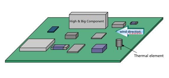
1. Thermal sensors (such as resistance capacitors, crystal vibration, etc.) should be as far away from high-temperature components as possible.
2. The thermal sensor shall be placed at the upper air outlet as far as possible, the high componentshall be placed behind the low-rise components, and the air duct shall be blocked along the direction of the least wind resistance. (Figure 1)
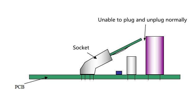
- The distance between components meets the requirements of operation space (such as: plug-in card).(Figure2)
- The metal parts or the components of metal shell with different properties cannot be touched. Ensure that the minimum distance of 1.0mm meets the installation requirements.
Reflow Soldering
General requirements for SMD components
- Fine pitch components are recommended to be placed on the same side of PCB, and heavy components (such as inductors, etc.) are recommended to be placed on the top side. Prevent dropping.
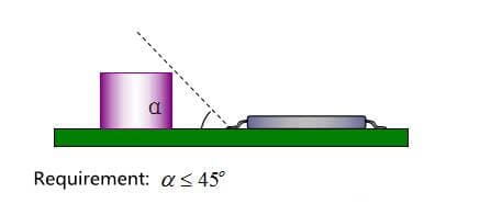
- The polar patches should be arranged in the same direction as far as possible to prevent the solder joint detection from being affected when the higher components are arranged next to the lower component Generally, the viewing angle should be less than 45 degrees. As shown in the figure 3.
- There should be a 2mm forbidden area around the CSP, BGA and other planar array components, and the best is 5mm forbidden area.
- In general, the layout of planar array components is allowed to be placed on the back; When there are array components on the back, it should not be within the projection range of 8mm forbidden area of array components on the front. As shown in the figure 4;

SMD component layout requirements
- The single side size of all SMDS is less than 50mm, and if it is beyond this range, it should be confirmed.
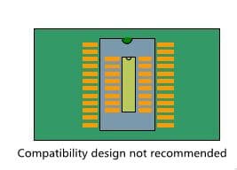
- It is not recommended that two surface mounted special-shaped pin components overlap as compatible design. Take SOP package componentas an example, as shown in the figure 5.
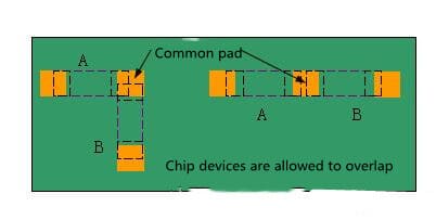
- Compatible substitution for two chip elements. The two components are required to be packaged in the same way. As shown in the figure 6
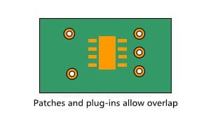
- Allow the THDand SMD to overlap the design when it is confirmed that the SMD pad and the solder paste printed on it will not affect the THD As shown in the figure 7.
Distance requirements between patch components:
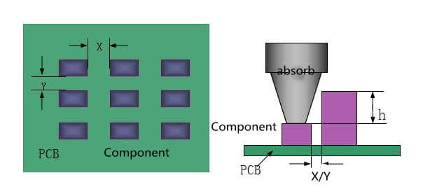
Same component: ≥ 0.3mm;
Heterologous component: ≥ 0.13 × H + 0.3mm (H is the maximum height difference of adjacent components around) (Figure 8)
List of SMT component distances for reflow process:
Note: the larger of the pad and the component body is the measurement body. The data in brackets in the table is the design lower limit considering maintainability.
Table 1 data sheet of component layout requirements
Unit(mm) | 0402~0805 | 1206~ 1810 | STC3528~ 7343 | SOT、SOP | SOJ、 PLCC | QFP | BGA |
0402~0805 | 0.40 | 0.55 | 0.70 | 0.65 | 0.70 | 0.45 | 5.00(3.00) |
1206~1810 | 0.45 | 0.65 | 0.50 | 0.60 | 0.45 | 5.00(3.00) | |
STC3528~7343 | 0.50 | 0.55 | 0.60 | 0.45 | 5.00(3.00) | ||
SOT, SOP | 0.45 | 0.50 | 0.45 | 5.00 | |||
SOJ, PLCC | 0.30 | 0.45 | 5.00 | ||||
QFP | 0.30 | 5.00 | |||||
BGA | 8.00 |
The distance between the fine pitch device and the plate edge where the transmission edge is located should be greater than 10 mm, so as not to affect the printing quality.
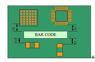
Suggestion: it is suggested that the distance between BARCODE frame and surface mount device should meet the following requirements. So as not to affect the quality of printing tin. See figure 9 and Table 2.
Table 2 Requirements for Distance Between Bar Code and Components of Different Packaging Types
Component type | Wing pin devices with pitch less than 1.27mm (such as SOP, QFP, etc.), plane array devices | Chip components above 0603 and other package components |
Minimum distance between bar code and device D | 10mm | 5mm |
Through hole reflow soldering device layout requirements
- For PCB with non transmission edge larger than 300 mm, the heavy components should not be placed in the middle of PCB. In order to reduce the influence of the weight of the plug-in device on the PCB deformation in the welding process, and the influence of the plug-in process on the devices that have been placed on the board.
- For convenience of insertion. The device is recommended to be placed close to the cartridge operation side.
- The distance between via reflow soldering device bodies is more than 10 mm.
- The distance between pad edge and transfer edge of through hole reflow soldering device is more than or equal to 10 mm, and the distance between pad edge and non transfer edge is more than or equal to 5 mm.
Wave Soldering
Layout requirements of wave soldering SMD devices
SMD for wave soldering
The chip resistance capacitance device and chip non exposed coil chip inductor with standoff value less than 0.15 are packaged in 0603 or above.
SOP device with pitch ≥ 1.27mm and standoff value less than 0.15mm.
Pitch ≥ 1.27mm, pin pad is exposed and visible sot device.
Note: the SMD height of all over wave soldering terminal pins is required to be ≤ 2.0 mm; The height of other SMD devices should be ≤ 4.0 mm.
The axial direction of SOP device should be consistent with the direction of wave crest. A pair of solder pads should be added at the end of the surge soldering for SOP devices. As shown in Figure 10.
The wave soldering direction of the device in SOT-23 package is defined according to the figure 11.
General principle of device spacing: considering the shadow effect of wave soldering, the device body spacing and pad spacing should be kept a certain distance.
Distance of the same type of component(Show as Figure 12)
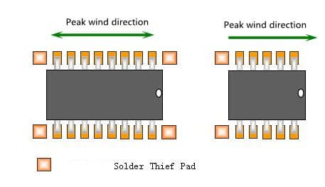
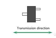
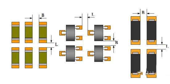
Table 3: layout requirements of the same type of devices
Package Size | Pad Spacing L(mm/mil) | Device Body Spacing B(mm/mil) | ||
| Mini Spacing | Recommended Spacing | Mini Spacing | Recommended Spacing |
0603 | 0.76/30 | 1.27/50 | 0.76/30 | 1.27/50 |
0805 | 0.89/35 | 1.27/50 | 0.89/35 | 1.27/50 |
≥ 1206 | 1.02/40 | 1.27/50 | 1.02/40 | 1.27/50 |
SOT | 1.02/40 | 1.27/50 | 1.02/40 | 1.27/50 |
Tantalum capacitor 3216, 3528 | 1.02/40 | 1.27/50 | 1.02/40 | 1.27/50 |
Tantalum capacitor 6032, 7343 | 1.27/50 | 1.52/60 | 2.03/80 | 2.54/100 |
SOP | 1.27/50 | 1.52/60 | — | — |
Distance of different types of components: distance between welding pad edge ≥ 1.0mm. See the requirements of Fig. 13 and table 4 for the distance of device body.
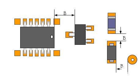
Table 4: Numerical table of different types of device layout requirements
Package Size (mm/mil) | 0603~1810 | SOT | SOP | Plug in Through Hole | Through Hole | Test Point | Solder Pad Edge |
0603~1810 | 1.27/50 | 1.52/60 | 2.54/100 | 1.27/50 | 0.6/24 | 0.6/24 | 2.54/100 |
SOT | 1.27/50 |
| 2.54/100 | 1.27/50 | 0.6/24 | 0.6/24 | 2.54/100 |
SOP | 2.54/100 | 2.54/100 |
| 1.27/50 | 0.6/24 | 0.6/24 | 2.54/100 |
Plug in Through Hole | 1.27/50 | 1.27/50 | 1.27/50 |
| 0.6/24 | 0.6/24 | 2.54/100 |
Through Hole | 0.6/24 | 0.6/24 | 0.6/24 | 0.6/24 | 0.3/12 | 0.3/12 | 0.6/24 |
Test Point | 0.6/24 | 0.6/24 | 0.6/24 | 0.6/24 | 0.3/12 | 0.6/24 | 0.6/24 |
Solder Pad Edge | 2.54/100 | 2.54/100 | 2.54/100 | 2.54/100 | 0.6/24 | 0.6/24 | 0.6/24 |
General layout requirements for THD devices
In addition to the special structural requirements, THD devices must be placed on the front.
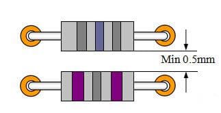
The distance between adjacent component bodies is shown in Figure 14.
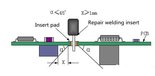
Meet the operation space requirements of manual welding and maintenance, as shown in Figure 15.
General requirements for wave soldering of THD devices
The device with pitch ≥ 2.0 mm and pad edge spacing ≥ 1.0 mm is preferred. On the premise that the device body does not interfere with each other, the edge spacing of adjacent device pads meets the requirements of figure 16.
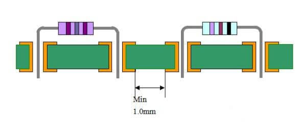
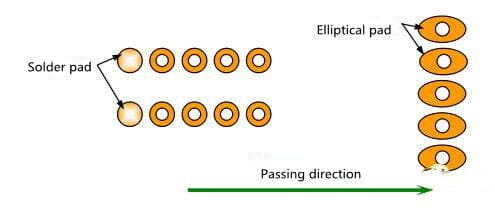
When the number of pins in each row of THD is large, the device is arranged in the direction of pad arrangement parallel to the incoming direction. When there are special requirements in layout and the direction of pad arrangement is perpendicular to the incoming direction, appropriate measures should be taken to expand the process window in pad design, such as the application of elliptical pad. For THD, when the edge spacing between adjacent pads is 0.6 mm-1.0 mm, elliptical pad or solder pad is recommended. (Show as Figure 17)

