Hole Design
1. Through Hole
Hole Spacing
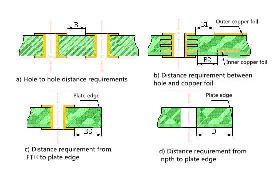
- The spacing between the hole and the hole disc is required: B ≥ 5MIL;
- The minimum distance between the hole plate and copper foil: B1-B2 ≥ 5MIL;
- The minimum distance between the metal hole (PTH) and the plate edge (hole to outline) ensures the distance between the welding pad and the plate edge: B3 ≥ 20MIL.
- The minimum distance between the wall of the non-metallic hole (npth) and the edge of the plate is recommended to be d ≥ 40mil.
(Show as Figure 1)
Forbidden zone of through hole
- The through hole cannot be located on the pad.
- There shall be no holes in the contact area between the metal shell and PCB extending outwards for 1.5mm.
2. Install Positioning Hole
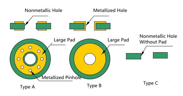
Selection of Hole Type
Show as Figure 2 and Table 1
Table 1: Preferred types of installation positioning holes
Working Procedure | Metal fastener hole | Non metallic fastener hole | Install Rivet Holes in Metal Parts | Install Rivet Holes in Nonmetallic Parts | Positioning Hole |
Wave Soldering | Type A | Type C | Type B | Type C | |
Non wave soldering | Type B |
Resistance Welding Design
1. Resistance welding design of conductor
It is generally required to cover resistance welding for wiring. PCB with special requirements can be made bare copper according to the needs.
2. Welding resistance design of holes
Via
The front and back sides of the resistance welding window setting of the through hole are hole diameter + 5MIL.
Hole installation
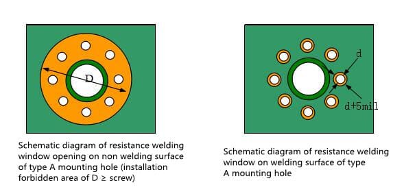
- In the forbidden area of the front and back sides of the metallized mounting hole, the window should be made by welding resistance.
- The size of the resistance welding window of the nonmetallic mounting hole with mounting copper foil should be consistent with the size of the installation forbidden area of the screw.
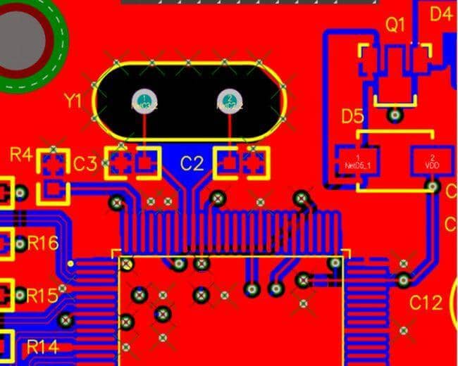
- It is recommended that the installation hole (microstrip pad hole) of the type of over wave soldering should be windowed for resistance welding. Show as figure 3.
Positioning hole
The front and back side of the nonmetallic positioning hole is 10 mil larger than the diameter of the window.
Design of through hole plug
- The holes that need plug holes do not have windows on both sides.
- The BGA vias of PCB that need over wave soldering or BGA / CSP with pitch < 1.0 mm adopt the method of Solder plug.
- If we want to add ICT test points under BGA, it is recommended to use dog bone shape to lead out test pad from via. The diameter of the test pad is 32 mil and the window is 40 mil.
- If the PCB has no wave soldering sequence and the pitch of BGA is greater than or equal to 1.0 mm, no hole plugging is performed. For the test point under BGA, the following methods can also be adopted: direct BGA through-hole is used as the test hole, without plugging the hole, t side is opened with 5MIL larger than the hole diameter, B side is opened with 32mil pad and 40mil window.
Solder mask design of pad
- Non solder mask defined is recommended.
- Due to the limitation of PCB manufacturers on solder mask alignment accuracy and minimum solder mask width, the solder mask window size should be more than 6mil larger than the pad size (3mil larger on one side), and the minimum solder mask bridge width should be 3mil. There must be solder bridge between pad and hole, between hole and adjacent hole to prevent solder from flowing out or short circuit.
Table 2: Recommended dimensions for resistance welding design
Item | Mini Value (mil) |
Dimension of plug-in pad resistance window (A) | 3 |
Size of solder bridge between wiring and plug-in (B) | 2 |
SMD pad solder mask window size (C)) | 3 |
Size of solder bridge between SMD pads (D) | 3 |
Solder bridge between SMD pad and plug in (E) | 3 |
Solder bridge between insert pads (F) | 3 |
Solder bridge between insert pad and via (G) | 3 |
Size of welding bridge between over hole and through hole (H) | 3 |
- SMD with lead spacing ≤ 0.5mm (20MIL), or edge spacing between pads ≤ 10mil can adopt the whole resistance welding window mode.
- Resistance welding window is recommended for copper paving for heat dissipation.
Resistance welding design of gold finger
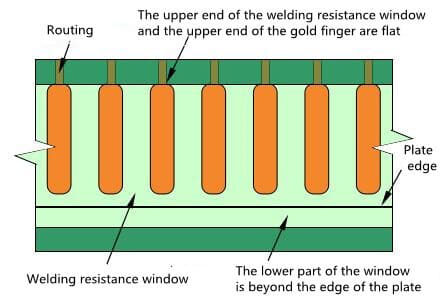
The whole window should be opened for the welding resistance of the gold finger, the upper end should be flush with the upper end of the gold finger, and the lower end should exceed the plate edge under the gold finger. As figure 4.
