For people who study electronics, it is natural to set up test points on the circuit board. But for people studying machinery, they might ask what are the test points. Maybe I’m still a little confused. I remember that when I first worked as a process engineer in a PCBA processing plant, I asked many people what are test points.
Basically, the purpose of setting test points is to test whether the components on the PCB meet the specifications and solderability. For example, if you want to check whether there is any problem with the resistance on a circuit board, the easiest way is to measure with a multi-meter. You can know it by measuring both ends.
However, in mass production factories, there is no way for you to use an electricity meter to slowly measure whether each resistance, capacitance, inductance, and even IC circuits on each board are correct. So there is the ICT (In -Circuit-Test) automated test machine. It uses multiple probes (generally called “Bed-Of-Nails” fixtures) to simultaneously contact all the parts on the board that need to be measured. Then the characteristics of these electronic parts are measured sequentially through the program control with sequence as the main and side-by-side method. Usually, it only takes about 1 to 2 minutes to test all the parts of the general board. It depends on the number of parts on the circuit board. It is determined by the parts. The more parts, the longer test time.
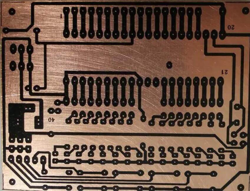
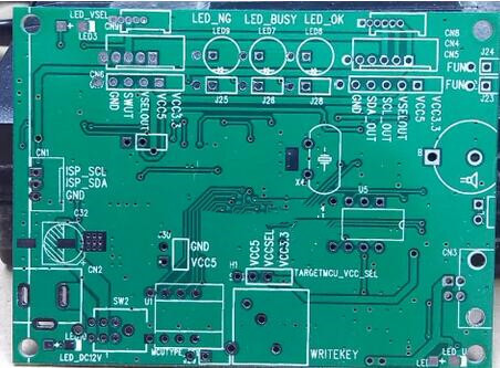
If these probes are allowed to directly contact the electronic parts or their welding feet on the board, it is likely to crush some electronic parts. On the contrary, it is just the opposite. So smart engineers invented “test points”, which lead out a pair of small round points on both ends of the parts without mask. There is no mask on it, which allows the probe to contact these small points instead of directly contacting the electronic parts to be measured.
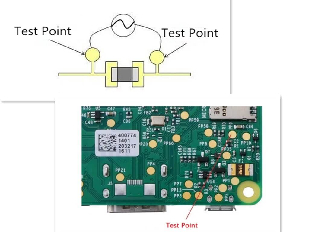
In the early days of traditional plug-in (DIP) on circuit boards, it was true that the solder pins of parts were used as test points. Because the solder pins of traditional parts were strong enough to be not afraid of pin pricking. But there were often misjudgments of poor contact of probes. Because the ordinary electronic parts were wave welded After eating tin, a layer of residual film of solder paste flux is usually formed on the surface of SMT solder. This film has very high impedance, which often leads to poor contact of the probe. Therefore, at that time, it is often seen that the test operators of the production line often blow desperately with the air gun, or wipe the places that need to be tested with alcohol.
In fact, the test points after wave soldering will also have the problem of poor contact with probes. After SMT became popular, the situation of misjudgment of test was greatly improved. The application of test points was also given great responsibility. Because the parts of SMT are usually very fragile and can’t bear the direct contact pressure of test probe. The test point can’t be directly connected to the parts and welding feet by using the test point. It not only protects the parts from damage, but also indirectly greatly improves the test results reliability. The misjudgment situation is less.
With the development of science and technology, the size of printed circuit boards is becoming smaller and smaller. It is hard to squeeze so many electronic parts on the board. The problem that test points occupy the space of circuit boards is often drawn between the design end and the manufacturing end. The appearance of the test point is usually round, because the probe is also round. It is better to produce and it is easier to make the adjacent probe close to a point, so that the density of needle implantation can be increased.
There are some mechanical limitations on the use of needle bed for circuit testing. For example, the minimum diameter of probe has certain limit, and the needle with too small diameter is easy to break and damage.
There are also some restrictions on the distance between pins. Because each pin should come out of a hole, and a flat cable should be welded at the back end of each pin. If the adjacent holes are too small, besides the problem of short circuit between pins and pins, interference of flat cable is also a big problem.
Some high parts cannot be planted next to them. If the probe is too close to the high part, it will be at risk of damage to the high part. In addition the parts are high, the holes on the needle bed base of the test fixture should be avoided, and the needle cannot be planted indirectly. Test points for all the parts below which the circuit board is becoming increasingly difficult to accommodate.
As the board is smaller and smaller, the storage and waste of test points are repeatedly discussed. There are some methods to reduce test points, such as net test, test jet, boundary scan, JTAG, etc,; There are other test methods to replace the original needle bed test, such as AOI and X-ray. But at present, each test seems to be unable to replace ICT by 100%.

