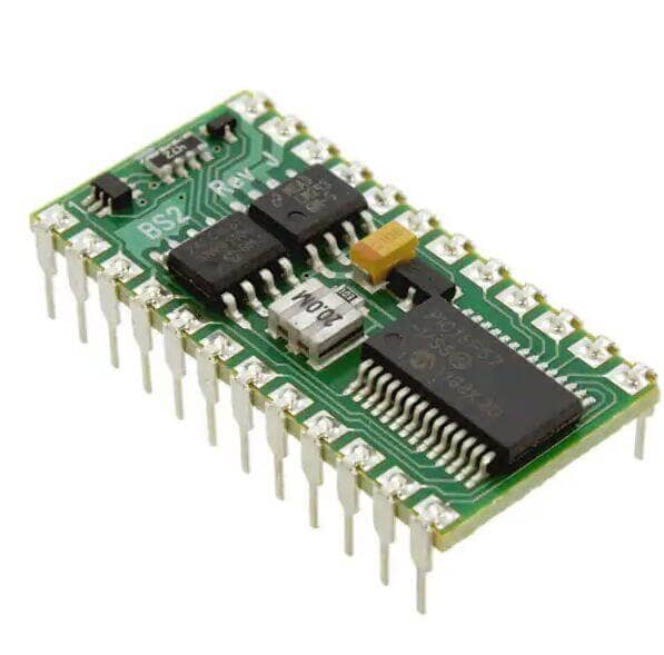
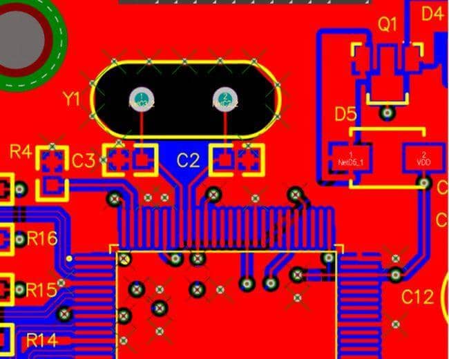
A printed Circuit Board (PCB for short), also known as the circuit board, PCB board, aluminum substrate, high-frequency board, ultra-thin circuit board, ultra-thin circuit board, printed (copper etching technology) circuit board, etc., is an important Electronic components are supports for electronic components and providers of circuit connections for electronic components. Traditional circuit boards use the method of printing etching resist to make circuit lines and graphics, so they are called printed circuit boards or printed circuit boards. Due to the continuous miniaturization and refinement of electronic products, most current circuit boards are made by attaching etch resist (lamination or coating), after exposure and development, and then etching to make circuit boards.
The principle of the circuit board
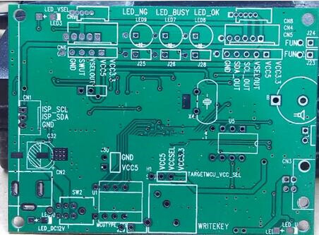
The circuit board mainly comprises pads, vias, mounting holes, wires, components, connectors, filling, electrical boundaries, etc. Common layer structures include Single Layer PCB, Double Layer PCB, and Multi-Layer PCB. The main functions of each component are as follows:
- Pad: Metal hole for soldering component pins.
- Vias: There are metal vias and non-metal vias, among which metal vias are used to connect component pins between layers.
- Mounting hole: used to fix the circuit board.
- Wire: The electrical network copper film used to connect the pins of components.
- Connectors: Components used for connection between circuit boards.
- Filling: Copper cladding for the ground network, which can effectively reduce the impedance.
- Electrical boundary: used to determine the size of the circuit board, and all components on the circuit board cannot exceed the boundary.
Working principle
Use the base insulating material to isolate the surface copper foil conductive layer, so that the current flows in various components along the pre-designed route to complete functions such as work, amplification, attenuation, modulation, demodulation, and encoding.
PCB Board Generation
There are three most common methods of Printed Circuit Board (PCB) board generation:
1. Subtractive method
There are two methods of subtraction, one is to remove the excess copper-clad layer by etching, and the other is to remove the excess copper-clad layer by engraving machine. The former is the most important method for PCB board production at present.
2. Addition method
The conductive material is selectively deposited on the substrate without copper foil to form a printed circuit board PCB with conductive patterns. There are silk screen electroplating methods, pasting methods, etc. However, this PCB manufacturing method is currently the only one in China. It is rare, so generally, PCB manufacturing methods are subtractive.
3. Semi-additive method
The circuit board semi-additive method is a combination of the above two.
PCB manufacturing is a very complicated process. Let’s learn about the issues that should be addressed during the PCB etching process.
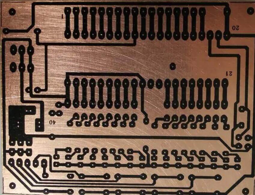
PCB Etching
Reduce side etch and edge, improve etch coefficient
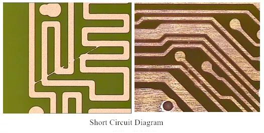
The side erosion produces a ledge. Generally, the longer the printed board is in the etching solution, the more serious the side etching will be. Side etching seriously affects the accuracy of printed wires, and severe side etching will make it impossible to make fine wires. When the side etching and the edge are reduced, the etching coefficient increases, and a high etching coefficient indicates the ability to maintain thin wires, so that the etched wires are close to the size of the original image. Plating etch resists whether tin-lead alloys, tin, tin-nickel alloys, or nickel, overburden can cause short circuits in the wires. Because the protruding edge breaks off easily, an electrical bridge is formed between the two points of the wire.
Influencing factors of side erosion
1. Etching method: Soaking and bubbling etching will cause larger side erosion, while splash and spray etching will cause smaller side erosion, especially spray etching has the best effect.
2. Types of etching solutions: different etching solutions have different chemical components, etching rates, and etching coefficients are also different. For example, the etching coefficient of acidic copper chloride etching solution is usually 3, and the etching coefficient of alkaline copper chloride etching solution can reach 4. Recent studies have shown that nitric acid-based etching systems can achieve almost no undercutting, and the sidewalls of etched lines are nearly vertical. Such etching systems are under development.
3. Etching rate: slow etching rate will cause serious side erosion. The improvement of etching quality has much to do with accelerating the etching rate. The faster the etching speed, the shorter the time the board stays in the etching solution, the smaller the amount of side etching and the etched graphics are clear and tidy.
4. The pH value of the etching solution: When the pH value of the alkaline etching solution is high, the side erosion will increase. In order to reduce side erosion, the general pH value should be controlled below 8.5.
5. Density of the etching solution: If the density of the alkaline etching solution is too low, the side erosion will be aggravated. Using an etching solution with a high copper concentration reduces side erosion.
6. Thickness of copper foil: It is best to use (ultra) thin copper foil to etch thin wires with minimum side erosion. And the thinner the line width, the thinner the copper foil thickness should be. Because the thinner the copper foil, the shorter the time in the etching solution, and the smaller the amount of side etching.

