Because the manufacturing process of printed circuit board is complex and the process is cumbersome, there are many quality defects in its manufacturing process, which seriously affects the quality of the final product. In order to reduce the unqualified rate of PCB and effectively control the quality defects in the production process, the main quality defects in the main manufacturing processes of PCB are briefly analyzed, so as to provide the necessary theoretical basis for solving the defects in the actual production. Following we will discuss the different types of short and open circuits.
Characteristics and Causes of Different Types of Short Circuits
Base copper short circuit
The utility model is characterized in that the copper surface foring a short circuit between two lines is significantly lower than the copper surface of the line, which may be a single short circuit or a large number of short circuits. The reason for the formation is that the dry film is not completely faded in the film removal process of etching, or the base copper is not etched during etching because the dry film chips are pasted on the plate surface.
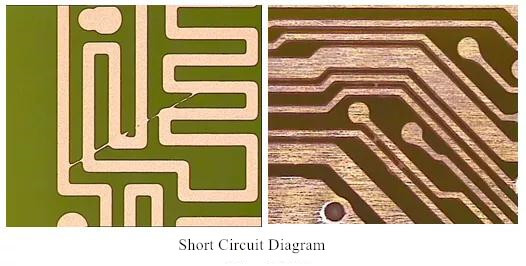
Electroplating short circuit
The utility model is characterized in that the copper surface forming the short circuit and the copper surface of the line are of equal height, which may occur as a single short circuit or a large number of short circuits. The reason is that the dry film breaks down because of the long time of plating or the violent stirring of solution. Copper and tin lead alloy are coated in the area covered by the dry film, and the short circuit is formed after etching.
Thin wire short circuit
It is characterized by a very thin copper wire between two wires to form a short circuit, and the width of the thin wire is 0.025 ~ 0.075mm. As long as the environmental control is not good during exposure, such as hair or other fine fibers falling on the board surface, resulting in a small dry film not exposed during exposure, and a short circuit is formed after the electroplating time is completed. A thin wire short circuit may also be a repetitive short circuit. But not much, because the production department will clean the exposure glass every time a certain plate is exposed.
Pit short circuit
It is characterized in that a small pit can be clearly seen in the area where the line defect is formed, and this short circuit is caused by the small pit. The reason is that pits are formed when the multilayer board is pressed or there are pits on the substrate. Because of the existence of pits, there is a gap between the dry film and the copper surface when sticking the dry film. Therefore, the pits are also electroplated during pattern electroplating, and a short circuit is formed after etching.
Insufficient etching
Generally, more or less copper like clouds can be seen in the large copper free area, with small thickness. In the observation line area, the short circuit is relatively long and continuous, and the short circuit copper surface is also lower than the line surface, which is caused by the low concentration of liquid medicine during etching or the set etching speed and time.
Scratch short circuit
It is characterized by more short circuits along a copper wire (not necessarily a straight line). The short circuit is also caused by this copper wire, and there are scratches along a certain direction. The reason is that the dry film is scratched or scratched by mechanical or human reasons after exposure and before electroplating (it can still be reworked before electroplating), and a short circuit is formed after electroplating and etching.
Characteristics and Causes of Different Types of Open Circuit
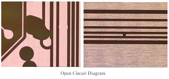
Repetitive open circuit
The utility model is characterized in that the same open circuit occurs in almost the same place of each plate, which is repeated for many times, and the number of exposed negatives is the same. The reason is that there are defects at the same position as the open circuit of the board on the exposure negative. In this case, the exposure negative must be scrapped, and the AOI detection of the first and last board during exposure shall be strengthened to ensure that the first board is correct before exposure.
Notch open circuit
The characteristic of this open circuit is that there is a gap on a conductor, and the remaining linewidth is less than 1 / 2 or equal to 1 / 2 of the normal linewidth due to the gap. Usually, the position is fixed and repeats for many times. The reason for its formation is that there is a defect on the exposure film, so there is also a gap in the wire at the same position of the board. The elimination method is to replace the exposure negative and strengthen the AOI detection in the exposure process.
Vacuum open circuit
In a certain area, several wires are getting thinner and thinner (gradually thinner), some form an open circuit, some do not have an open circuit, but they have to be scrapped because the wires are too thin (less than the minimum line width required by the customer). The reason for this defect is that the exposure film is not in close contact with the dry film, and there is air in the middle, that is, the vacuum pumping is not good after the exposure table is closed, and the vacuum degree can not meet the requirements, resulting in thinning or open circuit of the wire during exposure.
Scratch open circuit
The utility model is characterized in that the trace of the wire scratched by external force can be clearly seen, which also causes an open circuit. The reason is that the wire is scratched due to improper operation (such as the wrong method of holding the board, carelessness, etc.) or the machine, resulting in an open circuit.
Because the causes of outer circuit defects are complex, many situations are possible, which are not listed here, but most defects occur in materials such as copper clad laminate, film and dry film, or abnormalities occur in processes such as exposure, development and etching.


