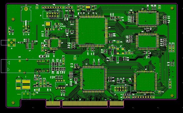
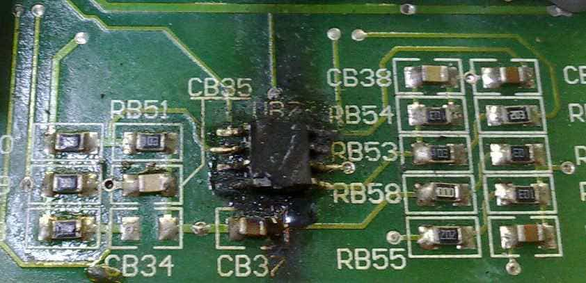
In PCB design, we always encounter this and that problem. This article summarizes 8 frequently asked questions you might come across. We discussed, and hope to help you.
Q1: Two characteristic impedance formulas are often referred to:
- Microstrip
Z={87 / [sqrt (Er +1.41)} ln [5.98H/ (0.8W+T)]
W— The width of the line
T — The thickness of copper skin of the line
H — The distance from the line to the reference plane
Er — The dielectric constant of PCB material.
This formula must be applied in the case of 0.1 < (W/H) < 2.0 and 1< Er < 15.
- Stripline
Z=[60/sqrt (ER)) ln{4h / [0.67 π (T+0.8W)]}
H — The distance between the two reference planes and the routing is in the middle of the two reference planes.
This formula can only be applied in the case of W/H < 0.35 and T/H < 0.25.
Q2: Can The Difference Signal Line be Grounded in The Middle?
The difference signal is usually not grounded. Because the most important point of the application principle of differential signal is the advantages of using the coupling between differential signals. Such as flux cancellation, noise immunity, etc. If ground wire is added in the middle, the coupling effect will be destroyed.
Q3: Does the Design of Rigid-flex Board Require Special Design Software And Specifications?
Rigid-flex and Flexible printed circuit boards can be designed by the general PCB design software. It is also produced to FPC manufacturers in Gerber format. Because of the different manufacturing process and general PCB, each manufacturer will have their own capability, such as the minimum line width, minimum line distance and minimum aperture (via), etc., In addition, copper sheet can be laid at the turning point of flexible circuit board to strengthen.
Q4: What is The Principle of Selecting The Grounding Point Between PCB And Shell Properly?
The principle of selecting PCB and enclosure grounding point is to provide low impedance path to return current and control the return current path by chassis ground. For example, the PCB layer can be connected with chassis ground by fixed screws near high frequency devices or clock generator, so as to minimize the area of the whole current loop and reduce electromagnetic radiation.

Q5: What Aspects Should The Board Debug Start With?
In terms of digital circuits, three things are determined in order:
- Confirm all power supply values are up to the design requirements.
Some multiple power systems may require some specification of the order and speed of the power supply to be connected. - Confirm all clock signal frequencies are working normally and there is no non monotonic problem on the signal edge.
- Confirm whether reset signal meets the specification requirements.
All of these are normal, the chip should signal the first cycle. Next debug according to the system operation principle and bus protocol.
Q6: How to Make There Are More Functions in The Design While The Board Size is Fixed?
Under the circuit board size is fixed, if more functions are needed in the design, usually we need to improve the density of PCB. However, this may lead to the mutual interference of the wiring and the too thin wiring, which will not reduce the impedance. Here we will introduce the skills in the design of high-speed (>100mhz) and high-density PCB.
Crosstalk interference is really important when designing high-speed and high density PCB, because it has a great influence on timing and signal integrity. Here are several points to note:
- The continuity and matching of the characteristic impedance of the line are controlled.
- Control the distance between the lines. The spacing commonly seen is twice the line width. The influence of the distance between the lines on the timing and signal integrity can be known through simulation, and the minimum distance that can be tolerated can be found. The results of different chip signals may be different.
- Select the appropriate termination mode.
- Avoid the same direction and the overlap of the two adjacent layers. Because the crosstalk is larger than that of the adjacent lines in the same layer.
- Blind/buried via is used to increase the area of the line. But the cost of PCB production will increase. It is really difficult to achieve full parallel and equal length in actual execution, but try to do it as much as possible.
- Differential termination and common mode termination can be reserved to mitigate the influence on the timing and signal integrity.
Q7: Why is LC Worse Than RC Filter Sometimes Although The filter at Analog Power Supply is Often LC Circuit?
The comparison of LC and RC filter effect must consider whether the selection of the frequency band and inductance value to be filtered out is appropriate. Because the inductance is related to the inductance value and frequency. If the noise frequency of power supply is low and the inductance is not large enough, the filtering effect may not be as good as RC. However, the cost of RC filter is that the resistance itself will consume energy and is inefficient. It is also necessary to pay attention to the power that the selected resistance can bear.
Q8: What is The Method of Selecting Inductance And Capacitance Value in Filtering?
Refer to the selection of inductance value, in addition to consider the frequency of noise you want to filter out, the ability to react to instantaneous current also needs to be considered.
If there is a chance that the output terminal of LC needs to output a large current instantaneously, too large an inductance value will hinder the speed of the large current flowing through the inductor and increase ripple noise. The capacitance value is related to the size of the ripple noise specification value that can be tolerated. The smaller the ripple noise value requirement, the larger the capacitance value. The ESR/ESL of the capacitor will also have an impact. In addition, if the LC is placed at the output of a switching regulation power, pay attention to the influence of the pole/zero generated by the LC on the stability of the negative feedback control loop.

