What is Impedance Circuit Board?
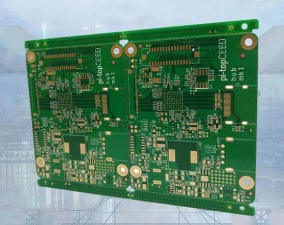
For PCB factories, boards with impedance lines are commonly known as impedance boards. The follow image is one of the common impedance boards.
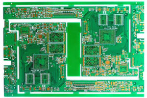
Generally, impedance is only made for high-speed boards, and the line width tolerance of impedance lines should be controlled to 5%-10% in the production process, while the tolerance of non impedance lines is 20%. Therefore, impedance production is difficult, and generally factories do not make impedance.
How to Choose The Produce Process of Impedance Circuit Boards?
Compression Structure
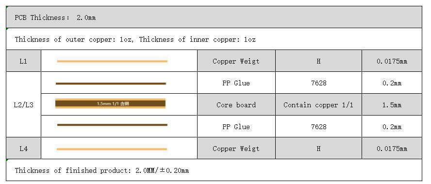
When placing an impedance board, we will find that we need to choose the compression structure (laminated structure) of the board. The lamination structure is divided into two types: the lamination specified by the customer and the lamination designed by the factory.
According to the lamination specified by the customer: this structure is generally selected when the engineer has calculated the impedance and has requirements for the thickness of the medium. At the same time, the structure drawing needs to be sent to the factory.
Design lamination according to the factory: the factory will give priority to calculate the analog impedance according to the conventional medium thickness. The figure below shows one of the laminated structures after the impedance simulation calculation of olinapcb.
| Recommended Impedance Linewidth | ||||
| Impedance Layer | Reference Layer | OHM | Line Width(mil) | Line Distance(mi)l |
| Top/Bottom | Top reference L2 Bottom reference L2 | 50 | 13 | / |
| 90 | 10 | 6 | ||
| 7.5 | 4 | |||
| 100 | 8 | 6.5 | ||
| 5.5 | 4 | |||
| L2/L3 | L2 reference L1&L3 L3 reference L4&L2 | 50 | 9.5 | / |
| 90 | 6.2 | 6.8 | ||
| 4.4 | 4.6 | |||
| 100 | 5.4 | 8.6 | ||
| 3.4 | 5.1 | |||
| Impedance calculation parameters
A. PP dielectric constant (PP model: 7628/1080/2313/2116, dielectric constant: 4.2) |
||||
What Are The Common Factors That Affect Impedance?
There are 4 common factors
1. Medium thickness: The thickness of double-sided board is only that of FR4 overall substrate board, and the thickness of multilayer board is PP sheet and core board.
2. Line width and line distance: The width of lines and the distance between lines will affect the impedance value.
3. Thickness of copper: The thickness of finished copper, usually 1oz, will also affect the impedance value if the surface copper is insufficient.
4. Dielectric constant: Here refers to the dielectric constant of ink and medium thickness.
What Information Does The Impedance Board Need to Provide to The PCB Factory?
- Identify which lines need impedance control in the form of documents or pictures.
- The calculated impedance and the line width and line distance of the laminated structure need to be provided, so that the factory can make special control during production to ensure that the finished product meets the impedance value.
- If you need to test by yourself, you need to note that you need to provide an impedance strip. You can use an impedance tester to measure the impedance value after you get the impedance strip. Those who are proficient in impedance can design impedance in the place where there is space in the board for later testing.

