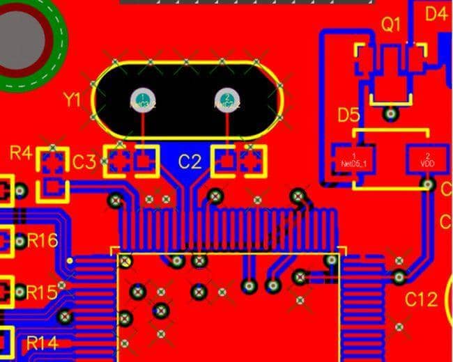
For PCB designers, creating a schematic symbol library and PCB packaging library is a very basic but very important work. Only by ensuring the accuracy of the schematic symbol library and PCB packaging library can we ensure the smooth development of PCB design. This book systematically introduces the methods and skills of schematic symbols and PCB packaging library, mainly including the basic knowledge of packaging library, packaging parameter analysis of component data manual, experience data of PCB packaging library engineering, review cases of schematic symbols and PCB packaging library, design of multi-platform schematic symbol library and PCB packaging library, conversion between PCB design documents and packaging library on multi-platforms Application of PCB 3D Packaging library and naming of PCB packaging.
As an excellent PCB layout engineer, good working habits will make your design more reasonable, performance better and production easier.
There are 7 good habits of PCB layout engineers.
- Learn Design Rules
In fact, not only advanced PCB design software needs to set wiring rules, but also some simple and easy-to-use PCB tools can set rules. After all, the human brain is not a machine, so it is inevitable that there will be negligence and mistakes.
So set some easily ignored problems into the rules and let the computer help us check to avoid making some low-level mistakes as far as possible.
In addition, a perfect rule setting can better standardize the later work. The more complex the board is, the more important the rule set is.
- Perform DRC (Design Rules Check) as Much as Possible
Although it takes only a short time to run the DRC function on PCB software, in a more complex design environment, you can save a lot of time as long as you always perform checks during the design process, which is a good habit worth keeping. Every routing decision is critical, and you can be prompted for the most important routing at any time by executing DRC.
- Draw the Schematic Diagram
Many engineers think that layout is more important. The schematic diagram is to generate a netlist for PCB inspection. In fact, the function of the schematic diagram will be greater in the subsequent circuit debugging process.
Whether it is to find problems or communicate with colleagues, or the schematic diagram is more intuitive and convenient. In addition, form the habit of marking in the schematic diagram, and mark the problems that should be noticed in the layout of each part of the circuit on the schematic diagram, which is a good reminder for yourself or others.
The hierarchical schematic diagram divides the circuits of different modules with different functions into different pages so that the workload can be significantly reduced whether it is reading the diagram or reuse in the future.
- Optimize PCB Layout
After drawing the schematic diagram and importing the netlist into the PCB, the anxious engineer can’t wait to put the devices in place and start pulling wires. In fact, a good PCB layout can make the pull wire work behind you easier and make your PCB work better.
Each board will have a signal path, and the PCB layout should follow this signal path as much as possible so that the signal can be transmitted smoothly on the board. People don’t like to go through the maze, and the signal is the same. If the schematic diagram is designed according to the module, the PCB can also be used.
The board can be divided into several areas according to different functional modules. Analog and digital are separated, power signals are separated, heating devices and susceptible devices are separated, larger devices should not be too close to the board edge, pay attention to the shielding of RF signals, etc… taking one more minute to optimize the PCB layout can save more time when pulling wires.
- Think More About Others
When designing PCB, consider the needs of end-users as much as possible.
For example, if you are designing a development board, you should consider placing more silkscreen information during PCB design, so that it will be more convenient to use it without looking up the schematic diagram or looking for the support of designers.
If the design is a mass-produced product, more consideration should be given to the problems encountered in the production line. The same type of devices should have the same direction as far as possible, whether the device spacing is appropriate, the process edge width of the board, etc.
The earlier these problems are considered, the less they will affect the later design, and can also reduce the workload of later support and the number of board changes. It seems that the time spent on design has increased, but in fact, it has reduced its subsequent workload.
When the board space signal allows, try to place more test points to improve the testability of the board, so as to save more time in the subsequent debugging stage and provide more ideas for finding problems.
- Communicate and Confirm With Customers Repeatedly
As excellent PCB layout engineers, we should learn to communicate effectively with customers.
For some important issues in layout, it is best to repeatedly communicate with customers for confirmation, such as the confirmation of packaging.
In particular, the positions of positive and negative electrodes, triodes, and structural connectors will directly affect the installation and positioning of boards in the later stage.
- Details Determine Success or Failure
PCB design is meticulous work, which requires care and patience.
Novice designers often make mistakes in details. Wrong device pins, wrong device packaging, reversed pin order, etc. some can be solved by flying wires, and some may turn a board into waste directly.
When painting the package, check it again. Before throwing the board, print out the package and compare it with the actual device. It’s not an obsessive-compulsive disorder to check it again. It’s just to avoid these easy low-level mistakes as far as possible.

