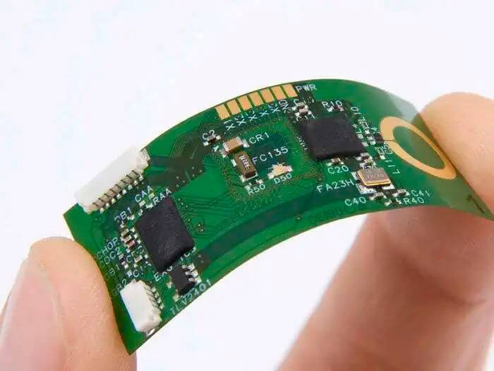
Because the manufacturing process of printed circuit board is complex and the process is cumbersome, there are many quality defects in its manufacturing process, which seriously affects the quality of the final product. In order to reduce the unqualified rate of PCB and effectively control the quality defects in the production process, the main quality defects in the main manufacturing processes of PCB are briefly analyzed, so as to provide the necessary theoretical basis for solving the defects in the actual production. Following we will discuss the lamination and drill process.
Analysis of Main Defects in Lamination Process
Delamination
Delamination refers to the separation between the layers of the substrate or between the conductive foil and the substrate. Delamination directly affects the reliability of printed boards. The obvious delamination can be observed directly with the naked eye without microscope analysis, that is, bubbles.
Causes of delamination after lamination of multilayer board
- The surface of copper foil or conductor copper is not properly treated before lamination, such as no oil removal, coarsening or blackening, and uneven browning.
- The surface of the semi cured sheet is not clean.
- The semi cured sheet is stored for too long.
- The pressing temperature and pressurization process control are abnormal, and the bubbles are not completely eliminated.
Interlaminar Dislocation
Interlaminar dislocation refers to the offset of the center of the connecting plate between layers.
Causes of interlayer dislocation
- Thermal expansion of inner material and resin flow of adhesive sheet.
- Thermal shrinkage in lamination.
- There is a large difference in thermal expansion coefficient between laminate and formwork.
Inclusion
Inclusion refers to metal foil or other foreign matters that have not been etched in the laminate.
Causes of interlayer inclusions
- Improper operation by staff.
- Excessive dust or suspended particles in the laminating environment.
- Abnormal setting of etching process control parameters or improper etching process.
Cavity
The cavity in the laminate is usually very small. In practice, when the plate thickness between two layers of conductors is 0.254mm, the maximum allowable diameter of the cavity is 0.076mm. The laminated cavity usually appears at the edge of the inner conductor or above and below the pad. After drilling, this cavity is likely to appear on the hole wall. Generally, there are holes with a diameter less than 0.076mm under the outer pad and conductor. However, there is a hole in the upper pressing plate of the hole wall. Due to the hole metallization, there is gas or other impurities in the hole metallization hole. The thermal shock during welding destroys the hole metallization and will affect the reliability of the printed board.
Causes of laminate voids
- There are too many chemical volatiles in the semi cured sheet.
- The moisture content of the resin system is too high and the humidity in the working room is high.
- The pressing die is not easy to exhaust.
Analysis of Main Defects in Drilling Process
Nail Head
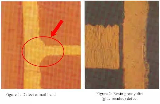
Because the copper foil drilled on the inner conductor pad of multilayer printed board is inclined outward, it is called nail head (as shown in Figure 1). There is no clear size requirement in most standards, but the maximum allowable nail head size for military multilayer printed circuit board is 50% of the thickness of copper foil. The existence of nail head indicates that the drilling quality of this multilayer printed circuit board has been greatly reduced, and the existence of nail head is also accompanied by epoxy resin greasy dirt.
Resin Greasy Dirt
After drilling, there is an epoxy resin coating on the inner conductor copper ring of multilayer printed board, so that the copper ring in the hole can not be fully exposed. This is usually called resin greasy dirt, and it is also called glue slag (as shown in Figure 2).
As resin greasy dirt seriously affects the connection between the hole wall metal and the inner copper ring, resin greasy dirt is not allowed on multilayer printed boards.
Causes of greasy dirt on nail head and resin
Since the thermal conductivity of the printed board substrate is lower than that of metal, a large amount of chip heat is generated during drilling, and most of the heat is transferred to the drill bit to reach a very high temperature. In addition to chip heat, the drilling friction between the drill bit and the hole wall also generates heat, which accelerates the wear of the drill bit. When drilling with a worn drill bit, it is easy to produce nail heads in the copper of the inner pad, Cause the unevenness of the hole wall. More seriously, due to the heat generated during drilling, the epoxy resin is softened by heating, and the softened resin sticks to the drill bit. It is easy to apply a layer of epoxy resin to the exposed copper ring when the drill bit feeds or retreats. It can be seen that this defect is related to the glass transition temperature of printed board materials, drill bit materials and geometric dimensions, drilling operation technology, etc.,
PadTearing
The so-called pad tearing refers to the tearing or cracking of the inner pad of multilayer printed board during drilling.
Causes of pad tear
This defect often occurs when a large nail head is generated, but it is mainly due to the large chip force generated by the drilling of the worn drill bit. When the peel strength between the laminate and the copper foil is low, the inner pad tear is more likely to occur.
Burr
After drilling, the copper foil protrusion on the two surfaces of the printed board around the hole is called burr. At present, the existing brush plate equipment can remove most of the burrs, but the extremely small burrs may not be removed completely. And it is possible to guide the burr into the hole and reduce the hole diameter. In serious cases, in order to remove burrs, the copper foil around the hole is damaged, resulting in poor contact between the hole wall and copper. Sometimes it can be broken by one circle.
Causes of burr
When the top angle of the drill bit is worn suddenly, the copper foil on both sides of the printed board can be burred. If the printed board is not pressed with the backing plates on the upper and lower sides, burr will also occur after drilling. The burr falls into the hole, which affects the metallization reliability of the hole.

