At present, there are mainly four kinds of stencil commonly used in SMT process according to manufacturing methods: chemical etching stencil, laser cutting stencil, electroformed stencil and mixed process stencil. OLINA PCB will briefly introduce the manufacturing methods of these four kinds of stencil.
Chemical Etching Stencil
Chemical etching is to use corrosive chemical solution to eliminate the metal corrosion at the position where the stainless steel sheet needs to be opened, so as to obtain the opening corresponding to the PCB pad and meet the stencil required for SMT chip processing and production. The manufacturing process is as follows:
Cutting appropriate size steel sheet → cleaning → coating photoresist material → UV exposure → development and drying → chemical etching → stripping photoresist material → cleaning and drying → inspection → net stretching → packaging
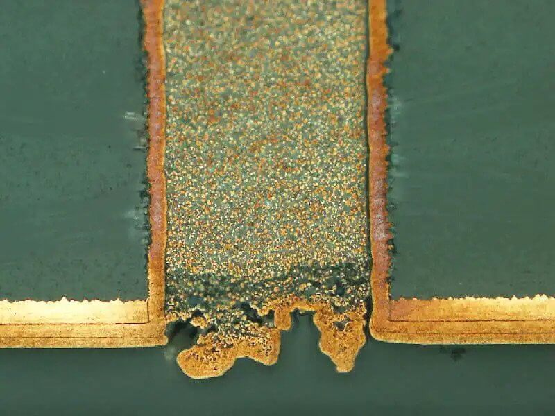
Because the chemical etching is to remove the metal from both sides of the steel sheet at the same time, the hole wall is smooth and vertical, but the metal may not be completely removed in the central part of the thickness of the steel sheet to form a conical shape, and the profile is in the shape of water leakage, which is not conducive to the release of solder paste. Therefore, etched stencil is generally not recommended for precision component assembly. Generally, etched stencil is not recommended for components with pitch less than 0.5mm or below 0402. Of course, for some large components or components with larger pitch value, the etched stencil has a greater cost advantage, and it can also meet the production quality requirements of many SMT chip processing plants.
Laser Cutting Stencil
High energy laser beam is used to cut and punch holes on stainless steel sheet to obtain the required stencil technology. The manufacturing process is as follows:
Data processing → laser drilling → polishing and electropolishing → inspection → net stretching → packaging
The principle of laser cutting is shown in the figure on the left, and the cutting process is finely controlled by the machine, which is suitable for the production of ultra small spacing holes. Because it is directly ablated by laser, the hole wall is straighter than that of chemical etching, and there is no middle cone shape, which is conducive to filling the mesh with solder paste. Moreover, due to the ablation from one side to the other, the hole wall will present a natural inclination angle, making the whole hole profile an inverted trapezoidal structure, and the taper is about half of the thickness of the steel sheet.
The inverted trapezoidal structure is conducive to solder paste release, and the small hole pad can get a better “brick” or “coin” shape, which is suitable for fine spacing or micro component assembly. Therefore, laser stencil is generally recommended for SMT assembly of precision components.
Electroformed Stencil
One of the most complex stencil manufacturing technology, using electroplating addition process to generate nickel sheet with required thickness around the pre-completed mandrel, has accurate size, and does not need post-treatment process to compensate the hole size and hole wall surface. The manufacturing process is as follows:
Coating photosensitive film on the substrate → making mandrel → electroplating nickel to form steel sheet around the mandrel → stripping and cleaning → inspection → stretching net → packaging
Electroformed stencil has smooth wall, inverted trapezoidal structure and the best solder paste release. It has good printing performance for micro BGA, ultra-fine pitch QFP and small chip components such as 0201 and 01005. Moreover, due to the characteristics of the electroforming process itself, a ring protrusion slightly higher than the thickness of the steel sheet is formed at the edge of the hole, which is equivalent to a “sealing ring” in solder paste printing. During printing, the sealing ring is conducive to the close fitting of the stencil with the pad or solder mask, preventing the leakage of solder paste to the outside of the pad. Of course, the stencil cost of this process is also the highest.
Mixed Process Stencil
In fact, the mixed process is commonly known as the ladder stencil manufacturing technology. Ladder stencil is to retain more than two kinds of thickness in a stencil, which is different from the stencil with only one thickness that we usually use. Its main purpose is to meet the different requirements of tin content for different components on the board. Ladder stencil manufacturing process is combined with one or two of the previous three kinds of stencil processing technology to complete a stencil. Generally speaking, many SMT chip processing plants will first use chemical etching method to obtain the steel sheet with the required thickness, and then use laser cutting to complete the hole processing.
There are two types of stepped stencil, step-up and step-down. The manufacturing process of the two types is basically the same. Whether it is up or down depends on whether the part to be changed is to increase or decrease the thickness. In order to meet the assembly requirements of local small spacing components on large plate (such as CSP on large plate), most components on the plate need more tin. For CSP or QFP components with small spacing, in order to prevent short circuit, it is necessary to reduce the amount of tin or avoid space. Therefore, step-down stencil can be used to thin the steel sheet at the location of small spacing components, Make the thickness of steel sheet here less than that of other positions. Similarly, for a small number of large pin components on some precision plates, due to the overall thickness of the steel sheet is thin, the amount of solder paste deposited on the pad may be insufficient, or for the through-hole reflow process, sometimes it is necessary to fill a larger amount of solder paste in the through-hole to meet the requirements of solder filling in the hole, which requires increasing the thickness of the steel sheet in the large pad or through-hole position of the stencil to increase the amount of solder paste deposition, This requires the use of step-up stencil. In the actual production, we need to determine which kind of stencil to choose according to the type and distribution of the components on the plate.
Olinapcb is a company providing PCB production and SMT stencil production services, which can provide you with high-quality product processing services.


