Datum Point Design
Classification
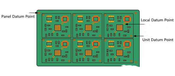
According to the position and function of the reference point on the PCB, it can be divided into: mosaic reference point, unit reference point and local reference point (as shown in Figure 6).
Benchmark Structure
Composition datum and unit datum
Shape / size: 1.0 mm diameter solid circle. Resistance welding window: the center of the circle is the center of the reference point, and the diameter is 2.0 mm. Protective copper ring: octagonal copper ring with the center as the center of the reference point and the distance between the opposite sides of 3.0 mm (as shown in figure 7-a).
Local datum point
Size / shape: 1.0 mm diameter solid circle. Resistance welding window: the center of the circle is the center of the reference point, and the circular area with a diameter of 2.0 mm. Protective copper ring: not required (Fig. 7-B).

Datum point position
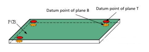
General principle: the reference point must be placed on the single board processed by SMT equipment; No reference point is needed for PCB that is not processed by SMT equipment.
The number of single-sided datum points is more than or equal to 3.
In SMD single-sided layout, only the datum points need to be placed on the surface of SMD components.
When SMD is arranged on both sides, the datum points should be placed on both sides; The two sides of the reference point, out of the mirror mosaic, the two sides of the reference point position requirements are basically the same(Figure 8)
Reference point of composition
Make-up needs to place make-up reference point and unit reference point.
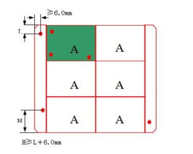
There are three reference points for plate making and three for unit. It is distributed in the shape of “L” on the edge of the plate. Try to stay away. See Figure 9 for the location requirements of the reference point.
When mirror symmetry is used, the reference points on the auxiliary side need to meet the requirement of overlap after flipping.
Datum point of unit plate
The number of datum points is 3, which is distributed in the shape of “L” on the edge of the plate, and the distance between the datum points is as far as possible. The distance between the center of the reference point and the edge of the plate must be greater than 6.0 mm. If the four edges cannot be satisfied, the transmission edge must at least meet the requirements.
Local datum point
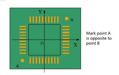
It is necessary to place local reference points for wing pin packaging devices with pin spacing less than or equal to 0.4mm and face array packaging devices with pin spacing less than or equal to 0.8mm.
The number of local datum points is 2. When taking the center of the component as the origin, the two datum points are required to be symmetrical (as shown in Figure 10).
Surface Treatment
Hot air leveling
Process requirements
The process is tin silver copper alloy covered on the surface of the PCB final exposed metal. The thickness of hot air leveling tin silver copper alloy coating is required to be 1 um to 25um.
Scope of use
Hot air leveling process is difficult to control the thickness of coating and the pattern of welding pad. PCB with fine spacing element is not recommended. The reason is that the flatness of the welding pad is high for the fine distance components; The hot air leveling process may cause PCB warping, and the surface treatment method is not recommended for ultra thin PCB with thickness less than 0.7mm.
Chemical nickel gold
Process requirements
The short name for chemical nickel gold system nickel leaching is 2.5um-5.0um for PCB copper metal surface, and 0.08um-0.23um for gold (99.9% pure gold) layer.
Scope of use
Because it can provide a relatively flat surface, this process is suitable for PCB with fine spacing elements.
Organic solderability protective film
Abbreviated as OSP, this process refers to the surface covering with specific organic matter on the exposed PCB copper surface, and is currently the only one.
The recommended organic protective layer is the enterprise’s Entek plus cu-106a, and its thickness is 0.2um-0.5um. It can provide very flat PCB surface, especially suitable for PCB with fine spacing elements.
Process Requirements for Output Documents
Assembly drawing requirements
It is required to have board name, version number, spelling method description and version information.
Requirements for steel mesh drawing
The board name and version number are required.
Requirements for drilling drawing
Plate name, version number, plate, surface treatment method, plate thickness, number of layers, interlayer arrangement, pore size, hole properties, dimensions and tolerance, and other special requirements.

