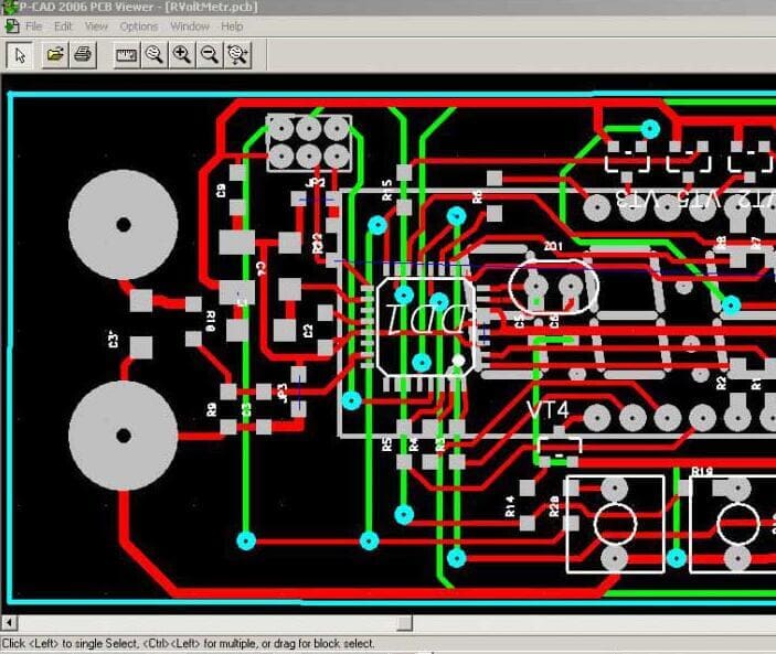
Lamination is the arrangement of the copper, and insulator layers that make up a PCB before the final layout of the board are designed. Managing a good press is not easy. The multi-layer structure increases the energy distribution capability of the board, reduces cross-interference, eliminates electromagnetic interference, and supports high-speed signals. While the press-fit level allows you to get multiple electronic circuits on one board through different layers of the PCB board, the structure of the PCB press-fit design offers many other advantages.
Advantages of PCB Lamination
- PCB layer lamination can help minimize circuit vulnerability to external noise, as well as minimize radiation, reducing impedance and crosstalk issues on high-speed systems;
- Good PCB lamination also contributes to efficient and low-cost final production;
- Correct PCB layer lamination can improve the electromagnetic compatibility of the project.
For single-layer or double-layer PCBs, board thickness is rarely considered. However, with the advent of multi-layer PCBs, the build-up of materials becomes more critical, and the final cost is the factor that affects the entire project. The simplest lamination can include a 4-layer PCB. More complex ones require professional sequential lamination. The more layers there is, the more freedom the designer has to break down the circuit, and the less likely he will get bogged down in “impossible” solutions. PCB overlay operations include the arrangement of copper and insulating layers that make up the circuit. The press fit you choose certainly plays an important role in the board’s performance in several ways.
For example, good layering can reduce the impedance of the board, limiting radiation and crosstalk. It also has a great influence on the EMC performance of the product. On the other hand, poor stack design can significantly increase the radiation and noise of the circuit.
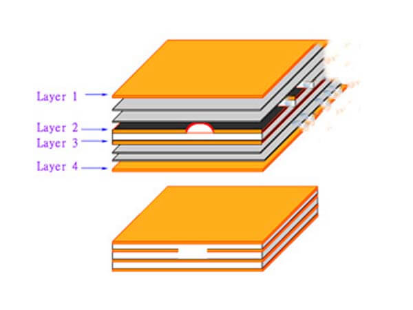
There are four important factors to consider when dealing with sheet stacking
- Number of layers
- Number and type of floor plans used
- Sorting and sequence of levels;
- The level of spacing.
Usually, few of these factors are considered other than those affecting the number of layers. Often, PCB designers are not even aware of the fourth factor.
Here are a few things to consider when deciding on the number of layers
- The number of signals to be routed and their cost;
- Working frequency;
- Whether the product complies with Class A or Class B emission requirements;
- Whether the PCB is in a shielded container;
- Whether the design team can implement EMC rules and regulations.
All factors are important and critical and should be considered equally. The use of multilayer boards with mass and power planes provides a significant reduction in radiated emissions. A generally used rule of thumb is that a four-layer board emits 15 dB less radiation than a two-layer board, all other factors equal.

