As an engineer, we often come across problems when we layout and route circuit board. According the experience, we summary some skills about the PCB layout and routing.
- Before PCB layout and routing, the layout of the components in the entire board needs to be set.
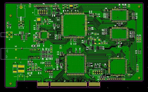
The shape and size of the board must be determined before the layout, which is related to the production cost and actual use in reality. After drawing the shape of the board, the main control chip is placed in the center of the board. Of course, this is not necessary. It is formulated according to the schematic diagram and actual use. The external thimble should be placed on the edge of the board. The power supply is placed in an open area of the board to facilitate heat dissipation. The real-time memory chip is placed around the main chip for easy storage.
- Arranging decoupling capacitors on the board, you need to arrange suitable capacitors in the right position.
Example: Add nearby the power port of the analog device, and need to use different capacitance values to filter out spurious signals of different frequencies.
- Multilayer design
The use of multi-layer boards can first provide a complete ground plane, and in addition can provide more signal layers to facilitate wiring. So when stacking, you can decide according to your actual situation.
- Multilayer board layout
Because the power supply and the ground plane are in the inner layer, be careful not to have a floating ground plane or power plane. In addition, make sure that the vias that hit the ground are indeed connected to the ground plane. Finally, add some test points for some important signals for convenience. Measure when debugging.
- Modular wiring can be used when wiring.
Divide all components into several groups for wiring. Of course, you need to do impedance simulation of the signal line to calculate the line width and the distance between the line and the ground before wiring. The power line needs to determine the line width according to the size of the current. Generally, the “line” is not used in the mixed-signal PCB, but the entire plane is used, so as to ensure that the loop resistance is minimized and there is a complete plane under the signal line.
- The proportional relationship between line width and matching via size
It is difficult to say that there is a simple proportional relationship, because the two simulations are different. One is surface transmission and the other is ring transmission. You can use the impedance calculation software of the via to calculate the relationship. Remember to keep the impedance of the via consistent with the impedance of the transmission line.
- AD conversion chip
If there are multiple AD conversion chips in the board, try to put several ADCs together and connect the analog and digital grounds at a single point under the ADC.
- Shield interference
A good PCB design requires as little as possible the emission of electromagnetic radiation to the outside, and also to prevent the interference of external electromagnetic radiation to itself. The best way is to shield to prevent external interference from entering. On the circuit, for example, when there is an INA, an RFI filter needs to be added before the INA to filter out RF interference.
- The copper setting of the circuit board
For the copper laying of the circuit board, if there is a complete ground plane and power plane inside, the top and bottom layers may not be coated with copper.

- Pin thickness of the device
Some devices have thinner pins, and some people worry about thicker traces on the PCB. Will it cause impedance mismatch after connection? It depends on the device. Moreover, the impedance of the device is generally given in the data sheet, and is generally not related to the thickness of the pin.
- Differential line
Differential lines can solve the problem of equal length by taking serpentine lines. Now most PCB software can automatically take equal length lines, which is very convenient.
- Device location
When designing a PCB, a good EMI/EMC design must take into account the location of the device, the arrangement of the PCB stack, the routing of important connections, and the selection of the device at the beginning of the layout.
- Serpentine routing
It has different functions because of different applications:
If the serpentine trace appears in the computer board, it mainly plays a role of filter inductance and impedance matching to improve the anti-interference ability of the circuit. The serpentine traces in the computer motherboard are mainly used in some clock signals, such as PCI-Clk, AGPCIK, IDE, DIMM and other signal lines.
If it is used in a general PCB board, in addition to the filter inductance, it can also be used as the inductance coil of the radio antenna and so on. For example, it is used as an inductor in 2.4G walkie-talkies.
- Blind or buried holes
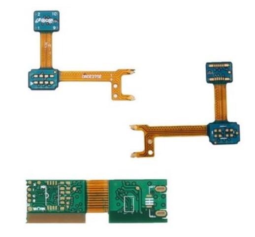
The use of blind holes or buried holes is an effective method to increase the density of multilayer boards, reduce the number of layers and the board size, and greatly reduce the number of plated through holes. However, in comparison, through holes are easy to implement in process and low cost, so through holes are generally used in the design.
- High-frequency signal wiring
Pay attention to the wiring of high-frequency signals:
The impedance matching of the signal line;
Space isolation from other signal lines;
For digital high-frequency signals, the effect of differential lines will be better;
- Number of vias
In the layout of the board, the number of vias, for low-frequency signals, vias does not matter, high-frequency signals try to reduce vias. If there are many lines, consider multi-layer boards;
- How to avoid noise introduced during wiring?
The digital ground and the analog ground should be grounded at a single point, otherwise the digital ground return will flow through the analog ground and cause interference to the analog circuit.
- How to consider the fusing current of PCB traces?
Refer to 0.15×line width (mm)=A, the maximum current at this time. The fusing current cannot be used as a budget during design. This is the cross-sectional area of the copper wire.


