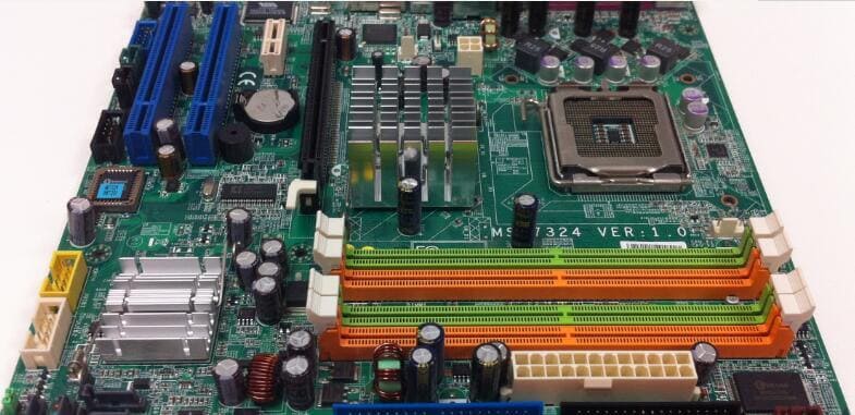
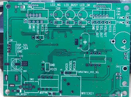
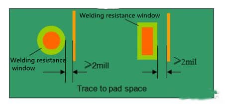
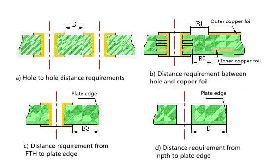
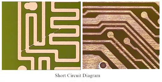
The PCB board is an important step in the electronic process. Almost all electronic products on the market are composed of PCB boards. What elements are there on a normal PCB board? Normally, it will generally include borders, vias, through holes, copper laying and so on.
Pad
It is the metal contact area used for soldering components, IC and other pins, usually on the surface of copper material.
Via
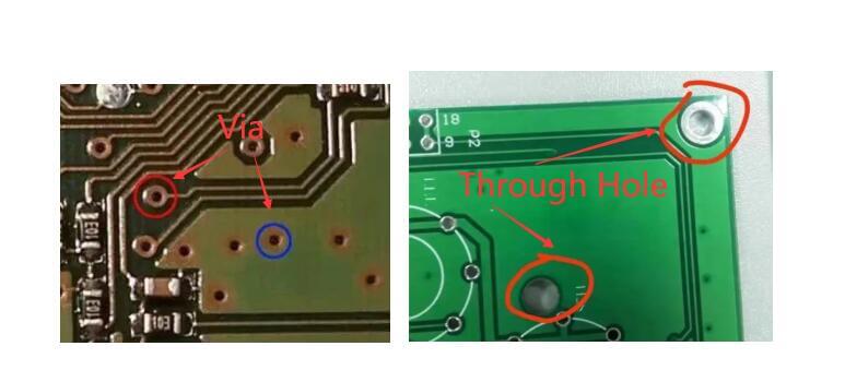
Vias are also called metallized holes. In double-layer boards and multi-layer boards, leads of different levels can be connected. It can be regarded as a common hole, which can maximize the lead space on the board.
Usually the via hole will be made into a circular pad shape, so the main parameters of the via hole are the outer diameter of the hole and the drilling size. Can maximize lead space on the deployment board.
Through Holes
Through-holes are divided into metal through-holes and non-metallic through-holes. Non-metallic through-holes are mainly used for fixing and are often used for screw holes without copper plating. The surface of the metal hole will be copper-plated and can be used for grounding and power supply.
Wire
It is used to connect the copper film of the electrical network of the component pins.
Connector
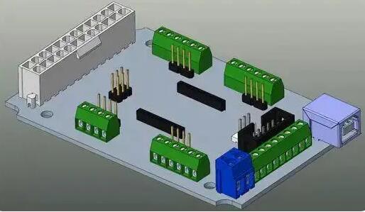
Components used for connection between circuit boards, such as connector terminals.
Filling
This is similar to filling, except that one is that filling is generally rectangular, while solid filling is of any shape.
Copper Laying
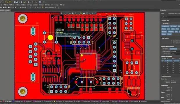
Use the unused space on the PCB as a reference plane, and then fill it with solid copper. These copper areas are also called pouring copper. Copper laying operation can effectively reduce impedance. However, not all boards need to be covered with copper, and it is necessary to choose whether to lay copper or not according to the actual situation. (generally the red part is copper)
Benefits of copper laying
(1) It can provide additional shielding protection and noise suppression for inner layer signals.
(2) It can improve the heat dissipation capacity of PCB.
(3) In the PCB production process, save the amount of corrosive agent.
(4) Avoid deformation and warping of the PCB due to the uneven stress of the PCB during reflow soldering due to uneven copper foil.
Disadvantages of copper laying
(1) The copper clad plane will be separated by the components on the surface. If there is a poorly grounded copper foil, EMI (electromagnetic interference) problems may occur.
(2) If the pins are also fully covered with copper, it will cause the heat to dissipate too quickly, and it will be more difficult in desoldering and rework soldering.
Electrical Boundaries (borders)
It is the actual size of the board, and all components on the board cannot exceed this boundary.

