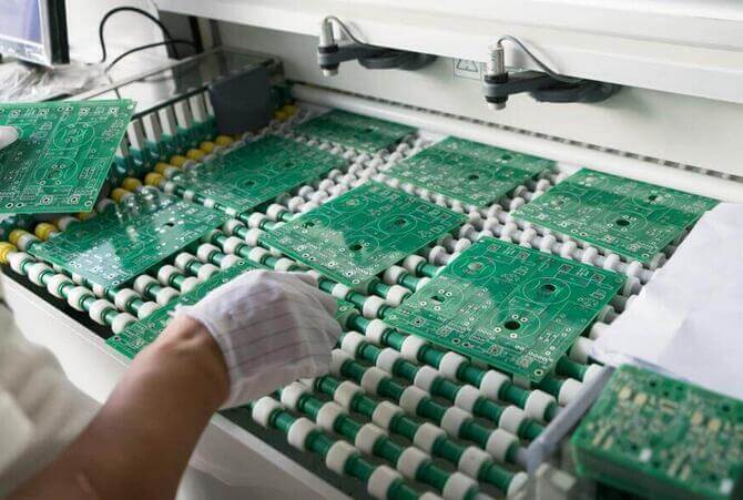
What’s Printed Circuit Board?
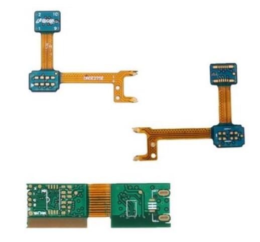
Printed circuit board is also known as PCB and is the provider of electrical connection of electronic components. It has a history of more than 100 years. Its design is mainly layout design. The main advantage of using circuit board is greatly reducing wiring and assembly errors, improving the level of automation and production labor rate. According to the number of PCB layers, it can be divided into single layer, double-sided board, four layer board, six layer board and other multilayer boards. Let’s take a look at printed circuit boards and integrated circuits.
The difference between PCB and Integrated Circuit Board (IC)
Integrated circuit generally refers to the integration of chips. For example, the Beiqiao chip on the motherboard and the CPU are all called integrated circuits. The original name is also called integrated block. The printed circuit refers to the circuit board that we usually see, as well as the soldering chip printed on the circuit board.
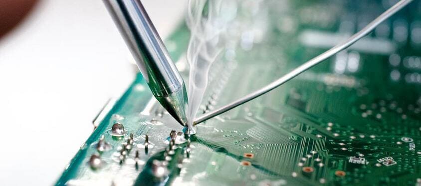
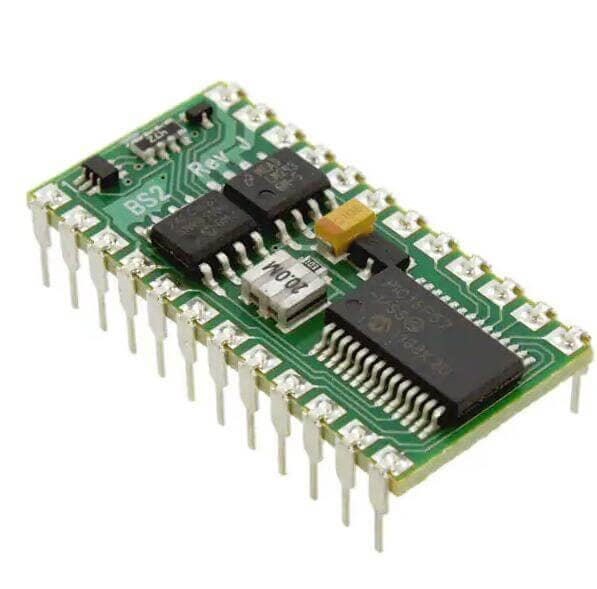
Integrated circuit (IC) is soldered on PCB board; PCB is the carrier of integrated circuit (IC). PCB is printed circuit board. Printed circuit board will appear in almost every kind of electronic equipment. If there are electronic parts in a certain equipment, printed circuit boards are inlaid on PCB of different sizes. In addition to fixing all kinds of small parts, the main function of printed circuit board is to make electrical connection between the parts above.
In short, integrated circuit is to integrate a general circuit into a chip. It is a whole. Once it is damaged internally, the chip will be damaged. PCB can solder components by itself. If it is damaged, components can be replaced.
Composition of PCB board
The current circuit board mainly consists of the following components:
Circuit and pattern: the circuit is used as a tool for conducting between the components. In the design, a large copper surface will be designed as the grounding and power layer. The route and the drawing are made at the same time.
Dielectric layer: used to maintain the insulation between the circuit and the layers, commonly known as the substrate.
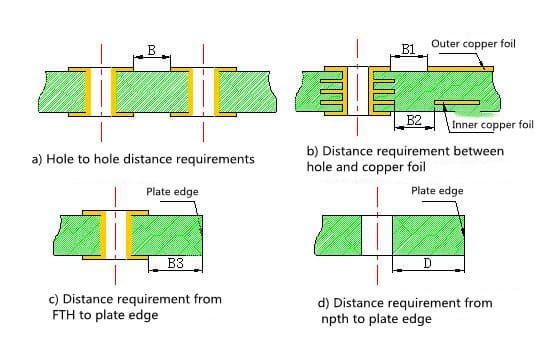
Through hole / via: the through hole can make more than two layers of lines conduct each other. The larger through hole is used as part plug-in. In addition, the non through hole (npth) is usually used for surface mounting positioning and fixing screw during assembly.
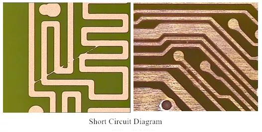
Solder resist / solder mask: not all copper surfaces need to be tinned, so the non tinned area will be printed with a layer of material (usually epoxy resin) to isolate the tinned copper surface, so as to avoid short circuit between non tinned lines. According to different processes, it can be divided into green oil, red oil and blue oil.
Legend / marking / silk screen: This is an unnecessary composition. Its main function is to mark the name and location box of each part on the circuit board, which is convenient for maintenance and identification after assembly.
Surface finish: because the copper surface is easily oxidized in general environment, it can not be tinned (poor solderability), so it will be protected on the copper surface to be tinned. The protection methods include HASL, ENIG, immersion silver, immersion tin and OSP. Each method has its own advantages and disadvantages, which are collectively referred to as surface treatment.
Characteristics of PCB
High density: For decades, PCB high density can develop with the improvement of IC integration and installation technology.
High reliability: Through a series of inspection, test and aging test, PCB can work reliably for a long time (generally 20 years).
Designability: For PCB performance requirements (electrical, physical, chemical, mechanical, etc.), PCB design can be realized through design standardization, standardization, etc., with short time and high efficiency.
Producibility: With modern management, standardization, scale (quantity), automation and other production can be carried out to ensure the consistency of product quality.
Testability: Established a relatively complete test method, test standards, various test equipment and instruments to detect and identify the PCB product qualification and service life.
Assemblability: PCB products are not only convenient for standardized assembly of various components, but also for automatic and large-scale mass production. At the same time, PCB and various component assembly parts can also be assembled to form larger parts, systems, and even the whole machine.
Maintainability: As PCB products and various component assembly parts are designed and produced in a standardized way, these parts are also standardized. Therefore, once the system fails, it can be replaced quickly, conveniently and flexibly, and the system can be restored quickly. Of course, there are more examples. Such as making the system miniaturization, lightweight, high-speed signal transmission and so on.
Characteristics of integrated circuit
Integrated circuit has the advantages of small volume, light weight, less lead and solder joint, long life, high reliability, good performance, low cost and easy to mass production. It is not only widely used in industrial and civil electronic equipment, such as radio recorder, television, computer and so on, but also widely used in military, communication, remote control and so on. Using integrated circuit to assemble electronic equipment, its assembly density can be increased dozens to thousands of times than transistor, and the stable working time of equipment can be greatly improved.
Integrated circuit is a kind of micro electronic device or component. The transistor, resistor, capacitor, inductor and other components needed in a circuit are interconnected by a certain process, which are fabricated on a small or several small semiconductor chips or dielectric substrates, and then packaged in a shell to form a micro structure with the required circuit function; All the components have been integrated in the structure, which makes the electronic components a big step towards miniaturization, low power consumption, intelligence and high reliability. It is represented by the letter “IC” in the circuit. The inventors of integrated circuits are Jack Kilby (GE based integrated circuits) and Robert Noyce (Si based integrated circuits).
Nowadays, most of the applications in semiconductor industry are silicon-based integrated circuits. It is a new type of semiconductor device developed in the late 1950s and 1960s. It is an electronic device that integrates the semiconductor, resistor, capacitor and other components needed to form a circuit with certain functions and the connecting wires between them on a small piece of silicon wafer through semiconductor manufacturing processes such as oxidation, photolithography, diffusion, epitaxy and aluminum evaporation, and then is welded and packaged in a shell. There are many kinds of packages, such as round shell, flat or dual in-line. Integrated circuit technology includes chip manufacturing technology and design technology, mainly reflected in the processing equipment, processing technology, packaging and testing, mass production and design innovation ability.

