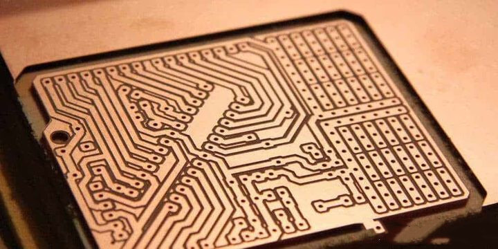
In PCB design, layout is an important part. The quality of the PCB layout result will directly affect the effect of the wiring, so it can be considered that a reasonable layout is the first step to a successful PCB design.
There are two layout methods, one is interactive layout, and the other is automatic layout.
Generally, interactive layout is used to adjust on the basis of automatic layout. In the PCB layout, the gate circuit can also be redistributed according to the wiring situation. Exchange the two gate circuits to make it the best layout for easy wiring. After the layout is completed, the design file and related information can be returned and marked on the schematic diagram. The relevant information in the PCB board is consistent with the schematic diagram. In the further the files and design changes can be synchronized. Simultaneously related to simulation The information is updated to enable board-level verification of the electrical performance and function of the circuit.
Considering the overall beauty and the success of a product, one must pay attention to the internal quality, and the other is to take into account the overall beauty. Both are more perfect to consider the product to be successful.
On a PCB board, the layout of components must be balanced, dense and orderly.
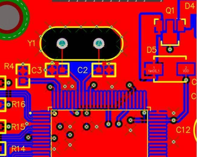
Layout Check:
- Does the size of the printed board match the size of the processing drawing?
- Can it meet the PCB manufacturing process requirements?
- Are there any positioning marks?
- Do components conflict in two-dimensional and three-dimensional space?
- Is the layout of the components sparse and orderly and neatly arranged?
- Is it all finished?
- Can the components that need to be replaced frequently be replaced easily?
- Is it convenient for the plug-in board to be inserted into the device?
- Is there an appropriate distance between the thermal element and the heating element?
- Is it convenient to adjust adjustable components?
- Is a radiator installed in a place where heat dissipation is required?
- Is the air flow unobstructed?
- Is the signal flow smooth and the interconnection shortest?
- Does the plug, socket, etc. contradict the mechanical design?
The Layout Principle of Common Components
- Arrange the position of each circuit unit according to the circuit flow, so that the layout is convenient for signal circulation, and the signal flow direction is kept as consistent as possible.
- On the premise of first satisfying the mechanical structure, in a given plane space, the basic principle of layout is to arrange the position of each circuit unit according to the circuit flow.
- Take the core component of each functional circuit as the center and lay out around it. The components should be arranged evenly, neatly and compactly on the PCB. Minimize and shorten the leads and connections between components. This is a more detailed explanation of how to properly lay out the separate components of resistors and capacitors under the premise of satisfying the first principle.
The Layout Principle of Special Components
- Try to shorten the wiring between high-frequency components as much as possible, try to reduce their distribution parameters and mutual electromagnetic interference. Components that are susceptible to interference should not be too close to each other, and input and output components should be kept as far away as possible.
- There may be a high potential difference between some components or wires, and the distance between them should be increased to avoid accidental short circuits caused by discharge. The components with high voltage should be arranged as far as possible in places that are not easily reachable by hands during debugging.
- Components weighing more than 15g should be fixed with brackets and then welded. Those components that are large, heavy, and generate a lot of heat should not be mounted on the printed circuit board, but should be mounted on the chassis bottom plate of the whole machine, and the heat dissipation problem should be considered. Thermal components should be far away from heating components.
- For the layout of adjustable components such as potentiometers, adjustable inductors, variable capacitors, and micro switches, the structural requirements of the whole machine should be considered. If it is adjusted inside the machine, it should be placed on the printed circuit board where it is convenient for adjustment; if it is adjusted outside the machine, its position should match the position of the adjustment knob on the chassis panel.
- The position occupied by the PCB positioning hole and the fixed bracket should be reserved.

