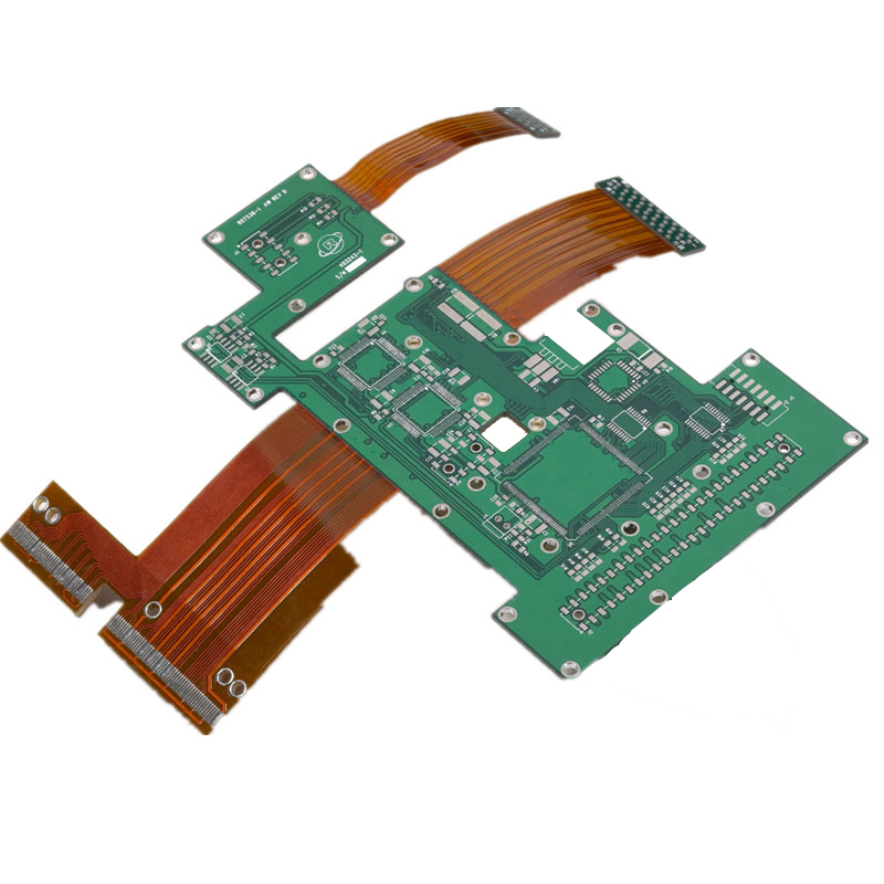
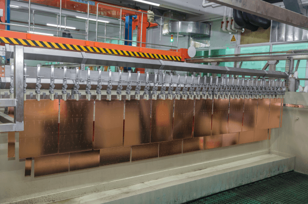
A multi-layer PCB is a printed circuit board with more than 2 layers. A double-sided PCB has two conductive layers on the top and bottom of the PCB substrate. A multi-layer PCB must have at least 3 conductive layers of conductive material or copper layers. All layers are interconnected with copper vias. It can be 4 layers, 6 layers, 8 layers, or even 40 layers.
The multi-layer PCBs are complex in design. The top and bottom layers look the same as a double-sided PCB, but with fixed layers on both sides of the core. All layers are compressed to form a single multi-layer PCB, where all layers are connected to each other through copper plated holes.
What Are The Applications of Multi-layer PCB?
Consumer Electronics
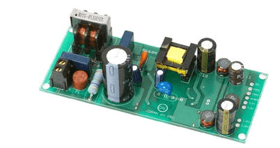
“Consumer electronics” is a broad term that includes many electronic devices under the general-purpose category that are directly relevant to ordinary users like you and me. Consumer electronics include: smartphones, smart watches, calculators, TV remotes, mp3 music players, toys, kitchen appliances, washing machines, electric kettles, electronic cigarettes, LED light bulbs, and energy savers, among others.
Computers and Equipment
Our world today is highly dependent on computers and automation. multi-layer PCBs are usually used in computers and related products, such as motherboards, graphics cards, eeprom, power supplies, keyboards, computer mice, ADCs, graphics processors, image processing circuits, etc.
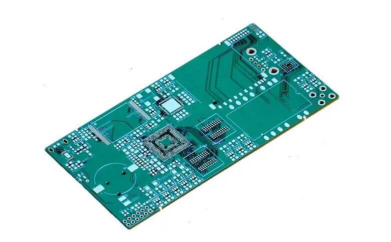
How to Identify Multi-layer PCB?
When calculating printed circuit board needs, consider the types of machines and equipment the PCB will be used in, and the requirements those machines/equipment will place on the board circuitry. Will these PCBs be used in high-tech, complex electronics, or in products with simpler functions? Other things to consider are the manufacturing costs of single-layer and double-layer PCBs versus multi-layer PCBs. If you want to have the highest capacity in today’s board technology, you will need to pay high manufacturing costs.
Lead time is something to consider when you are ordering large quantities of printed circuit boards. Lead times for one- and two-layer boards can vary from 8 to 14 days, depending on the size of the board area. However, delivery times can be as short as five days or as long as a month if you’re willing to pay more or less. With each additional layer, the lead time increases. PCBs in the range of 4 to 20 layers can have a lead time of 12 to 32 days, depending on whether you want the board size large or small.

