Factors to consider in PCB stack-up design
1. Hardware cost
The number of PCB layers is directly related to the final hardware cost. The more layers, the higher the hardware cost. Hardware PCBs represented by consumer products generally have the highest limit on the number of layers, such as notebook computer products. The number of layers of the motherboard PCB is usually 4~6 layers, rarely more than eight layers.
2. Outgoing lines of high-density components
High-density components represented by BGA package devices, the number of outgoing layers of such components determines the number of wiring layers of the PCB board.
3. Signal quality control
For PCB design, where high-speed signals are relatively concentrated, if the focus is on signal quality, it is required to reduce the wiring of adjacent layers to reduce crosstalk between signals. At this time, the number of wiring layers and the number of reference layers (Ground layer or The ratio of Power layer) is preferably 1:1, which will increase the number of PCB design layers; on the contrary, if the signal quality control is not mandatory, it can use the adjacent wiring layer scheme to reduce the number of PCB layers.
4. Schematic signal definition
The schematic signal definition will determine whether the PCB wiring is “smooth,” and a poor schematic signal definition will cause the PCB wiring to be unsmooth and the number of wiring layers to increase.
5. PCB manufacturer’s processing capability baseline
The stacking design scheme (stacking method, stacking thickness, etc.) given by the PCB designer must fully consider the PCB manufacturer’s processing capability baseline, such as processing process, processing equipment capability, commonly used PCBs Plate model, etc.
PCB stack-up design needs to seek priority and balance among all the above design influencing factors.
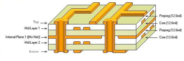
General Rules for PCB Stack-up Design
- The ground layer and the signal layer should be tightly coupled.
Itmeans that the distance between the ground layer and the power layer should be as small as possible. The thickness of the medium should be as small as possible to increase the capacitance between the power layer and the ground layer (if you do not understand here, you can think about the plate capacitor, the size of the capacitor is inversely proportional to the spacing). - Avoid being directly adjacent between the two signal layers.
Directly adjacent between two signal layers, which is prone to signal crosstalk and affects the circuit’s performance. - For multi-layer circuit boards, the signal layer should be adjacent to an internal electrical layer as much as possible.
For multi-layer circuit boards, such as 4-layer boards and 6-layer boards, it is generally required that the signal layer be adjacent to an internal electrical layer (ground layer or power layer) as much as possible. So that the large-area copper cladding of the internal electrical layer can be used. Shielding the signal layer can effectively avoid the crosstalk between the signal layers. - The high-speed signal layer is generally located between the two internal electrical layers.
This purpose is to provide an effective shielding layer for the high-speed signal on the one hand and to limit the high-speed signal to the two internal electrical layers on the other hand. Between layers to reduce interference to different signal layers. - Consider the symmetry of the stacked structure.
- Multiple grounded inner electrical layers can effectively reduce the grounding impedance.
Recommended Stacked Structure
- Lay the high-frequency traces on the top layer to avoid the introduction of inductive inductance due to the use of vias in the process of high-frequency traces. On the top layer isolator and the data lines of the transmit and receive circuits are directly connected with high-frequency traces.
- A ground plane is placed under the high-frequency signal line to control the transmission connection line’s impedance and provide a shallow inductance path for the return current to flow.
- Place the power plane under the ground plane. These two reference layers form an additional high-frequency bypass capacitor of approximately 100pF/inch2.
- Layout low-speed control signals on the bottom wiring. These signal lines have a large margin to withstand impedance discontinuities caused by vias, which allows for more flexibility.
Example of Four-layer Board Stack-up Design
If an additional power supply layer (Vcc) or signal layer is required, the additional second set of power supply/ground layers must be stacked symmetrically. This way, the laminated structure is stable, and the board will not warp. The power and ground planes of different voltages should be close together so that high-frequency bypass capacitors are added to suppress noise.

