Before printed circuit board design begins, designers should take some basic steps to ensure a successful project, such as management and scheduling. Time and resources must be allocated to the project, including buffers for design changes or bugs that require changes to the schematic and layout. All too often, PCB designers have to struggle to complete projects, resulting in missed plans, errors, or incomplete work. A circuit board starts with its design and layout. Let’s look at common printed circuit board issues in PCB design to avoid manufacturing delays.
PCB Design Common Problems
1. Component issues
Later in the series on common PCB issues, we will delve into component issues in more depth in an article. However, during the design phase, one of the main problems with assemblies is choosing the wrong part for convenience. Designers can easily reuse existing circuits or select library parts because it is familiar. The problem is when those parts are no longer viable due to price or availability or have become obsolete. Designers need to keep their libraries up to date and check the components they are using to avoid this problem.
2. Physical parameters
Layout teams typically adopt board outlines, material selections, or layer stack configurations because they are familiar. But material availability and price may change, and design requirements may favor different substrates. Board outlines may also change or need to be changed due to manufacturing constraints. To avoid such problems, confirming the board’s parameters with the manufacturer is best before starting the layout.
3. Part Placement
The PCB assembly footprint must be placed in the board design to reduce or eliminate manufacturability issues. This process is known as Design for Manufacturing or DFM, and if neglected, it can lead to a drastic drop in yield while overall costs skyrocket. Some DFM requirements that designers need to be aware of are spacing between components, between components and board edges, and between components and other board features. Allowing enough space around the test points is also necessary to ensure that the board can be automatically tested. The placement of heat-generating components should be considered to prevent thermal issues from affecting the board’s performance, and high-speed parts need to be placed for optimal signal integrity performance.
4. Traceroute
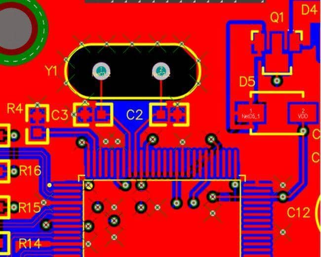
One of the most common design problems is incorrect trace width and spacing. Not only should designers work with their manufacturers to determine the correct trace width and copper weight, but these values must be entered into CAD design rules. A complete set of design rules and constraints will help avoid issues like controlled impedance routing, traces with higher current burn-through due to insufficient copper, poor signal integrity, and improper copper balance on board layers.
5. Power and ground planes
It is common for PCB designers to treat their power supply network as an afterthought or not consider it necessary. However, without a properly designed ground plane, the board can suffer from noisy signal integrity issues and radiate unwanted EMI. Again, the answer is to work with the manufacturer to determine the correct configuration and placement of planes in the ply stack. It is also important to design these planes so that signal return paths are not blocked and areas of different circuits (such as analog and ground) do not interfere with each other.
6. Whole system design
Designers are often so focused on their PCB designs that they forget that their boards are often part of a larger system. This lack of integration can lead to future problems when all system components come together. Wire harnesses may not match the corresponding connectors on the board, and switches and other human-machine interfaces may not be accessible. Technicians will not have the space needed for debugging and rework. Therefore, engineers must design for the entire system, not just the PCB in front of them.

