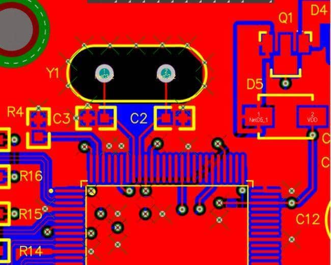
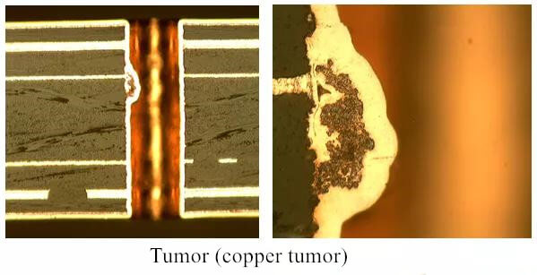
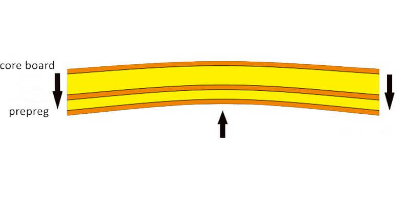
Ordinary PCB is usually made of copper foil and substrate, and the substrate material is mostly fiberglass (FR-4), phenolic resin (FR-3), and other materials. The adhesive is usually phenolic, epoxy, etc. During the PCB processing process, due to thermal stress, chemical factors, improper production processes, etc., or due to the asymmetry of copper paving on both sides during the design process, it is easy to cause the PCB board to warp to varying degrees.
Ceramic PCB Board
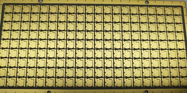
PCB ceramic substrate refers to a special process board in which copper foil is directly bonded to the surface (single or double-sided) of aluminum oxide (Al2O3) or aluminum nitride (AlN) ceramic substrate at high temperatures. The ultra-thin composite substrate produced has excellent electrical insulation properties, high thermal conductivity, excellent solderability and high adhesion strength, and can be etched with various patterns like a PCB board and has a large current carrying capacity. ability. Therefore, ceramic substrates have become the basic material for high-power power electronic circuit structure technology and interconnection technology.
The main materials of ceramic PCB substrate
Alumina (Al2O3)
Aluminum oxide is the most commonly used substrate material in ceramic substrates because it has higher strength and chemical stability than most other oxide ceramics in terms of mechanical, thermal, and electrical properties. It also has abundant raw materials and is suitable for various technologies. Manufactured in different shapes as well. According to the percentage of aluminum oxide (Al2O3), it can be divided into 75 porcelain, 96 porcelain, and 99.5 porcelain. Aluminum oxide content is different; its electrical properties are almost unaffected, but its mechanical properties and thermal conductivity vary greatly. Substrates with low purity contain more glass phases and have larger surface roughness. The higher the purity of the substrate, the smoother, denser, and lower the dielectric loss, but the higher the price.Beryllium oxide (BeO)
It has a higher thermal conductivity than metallic aluminum and is used when high thermal conductivity is required. It decreases rapidly after the temperature exceeds 300°C, but its toxicity limits development.Aluminum nitride (AlN)
Aluminum nitride ceramics have aluminum nitride powder as the main crystal phase. Compared with alumina ceramic substrates, the insulation resistance and voltage are higher, and the dielectric constant is lower. Its thermal conductivity is 7 to 10 times that of Al2O3, and its coefficient of thermal expansion (CTE) approximately matches that of silicon wafers, which is crucial for high-power semiconductor chips. Regarding the production process, the thermal conductivity of AlN is greatly affected by the content of residual oxygen impurities. Reducing the oxygen content can significantly improve the thermal conductivity. It is no longer a problem for the thermal conductivity of the current process production level to reach more than 170W/(m·K).
Based on the above reasons, alumina ceramics are still in a dominant position in the fields of microelectronics, power electronics, hybrid microelectronics, power modules, and other fields due to their superior comprehensive properties.
Ceramic PCB Classification
Ceramic PCBs in the electronics market are divided into three types based on the manufacturing method.
- High-temperature ceramic PCB
- Low-temperature ceramic PCB
- Thick film ceramic PCB
High-temperature ceramic PCB
As you know, high temperature is probably the most popular type of ceramic. Generally speaking, ceramic PCBs designed for high temperatures are usually considered high-temperature co-fired ceramic (HTCC) circuits composed of ceramic raw materials and solvents, mixed adhesives, plasticizers, lubricants, and alumina.
It is first made from ceramic raw materials, then the material is coated, and then the circuit trace is applied to tungsten or molybdenum metal. Finally, if circuit tracing is implemented, the board can be baked between 1600 and 1700 degrees Celsius for up to 48 hours after lamination. All HTCC bakes are performed in a gas environment, such as hydrogen.
Low-temperature ceramic PCB
Different from HTCC, low-temperature co-fired ceramic PCBs are made of crystal glass and an adhesive substrate combined with gold paste on a metal plate. The boards are then cut and laminated before being placed in a gas oven at approximately 900 degrees Celsius.
Moreover, low-temperature co-fired ceramic PCBs benefit through less warpage and progressive shrinkage tolerance. That is to say, compared with ceramic PCBs such as HTCC, ceramic PCBs have better mechanical strength and thermal conductivity. Therefore, when using heat dissipation products such as LED lights, the heat dissipation advantages of LTCC are advantageous.
Thick film ceramic PCB
In thick film ceramic PCB, the thickness of the conductor layer may exceed 10 microns but not exceed 13 microns. Generally speaking, the conductor layer is printed with silver or gold palladium on the surface of the ceramic PCB. That is to say, thick film ceramic PCB includes gold and dielectric paste, which is done on the ceramic substrate, and the paste and backing are carried out at a temperature of 1000 degrees Celsius or below after work. Therefore, most PCB manufacturers widely use thick film ceramic PCBs due to the high cost of gold conductor paste.
The main advantage of thick film ceramic PCB over traditional PCB is that thick film ceramic can protect copper from oxidation. So ceramic PCB manufacturers can place interchangeable conductors, semiconductors, conductors, capacitors, or resistors on the ceramic board. After completing the printing and high-temperature sintering process, all components on the board can be laser-trimmed to their desired values.
There is confusion about how many layers a ceramic PCB has, but the type of ceramic PCB determines it. The minimum number of layers for a ceramic PCB is two, but some may be added depending on the product’s characteristics.
Uses of Ceramic PCB
- High-power power electronic modules, solar panel components, etc.
- High frequency switching power supply, solid state relay.
- Automotive electronics, aerospace, military electronic products.
- High-power LED lighting products.
- Communication antenna, car ignition.
Ceramic Substrate Processing Capabilities
| Ceramic Substrate Processing Capabilities | |
| Layer | 1-6 layers |
| Product Types | Single & double layers, 3D dam |
| Produce Time | 2-4 weeks |
| Ceramic Substrate | Aluminum oxide, aluminum nitride, zirconium oxide, beryllium oxide, silicon nitride |
| Max PCB Size | 127*178 mm |
| Finished Board Thickness (mm) | 0.25, 0.3, 0.38, 0.5, 0.635, 0.8, 1.0, 1.2, 1.5, 2.0 |
| Shape Tolerance | ± 0.1 mm |
| Min Line Width/Line Spacing | 2 mil/2 mil |
| Finished Board Copper Weight | <127 µm |
| Bore Diameter Tolerance | PTH: ± 0.075 mm NPTH: ± 0.05 mm |
| Minimum Laser Drilling Diameter | 0.06 mm |

