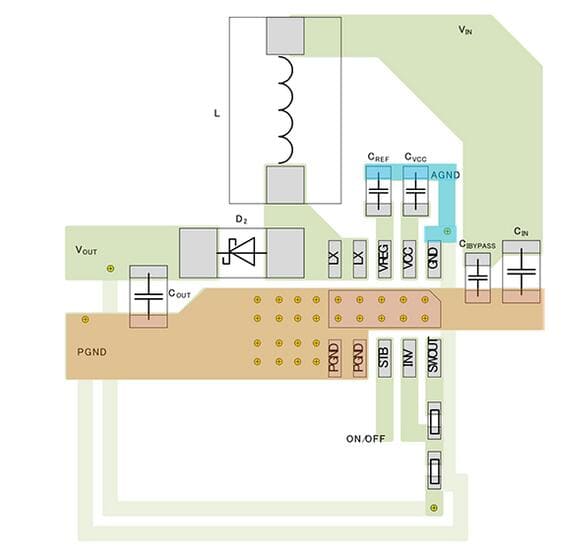
First of all, analog small signal grounding and power grounding must be separated.
In principle, the layout of power grounding does not need to be separated from the top layer with low wiring resistance and good heat dissipation. If the power supply is separated from the ground and connected to the back through the via, the loss and noise will deteriorate due to the influence of the via resistance and inductor. In order to shield, dissipate heat and reduce DC loss, the method of setting grounding layer in inner layer or back is only auxiliary grounding.
The figure above shows the layout of the circuit board in this example.
The figure below is an example of the basic layout of power ground (PGND, orange part) and analog small signal ground (agnd, light blue part) on the top floor.
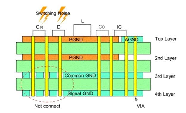
When the ground plane is designed in the inner layer or back of the multilayer circuit board, special attention should be paid to the power supply grounding with high frequency switching noise.
If the second layer has a power ground layer designed to reduce DC loss, use multiple vias to connect the top layer and the second layer to reduce the impedance of the power ground.
In addition, if there is a common ground on the third layer and a signal ground on the fourth layer, the connection between the power ground and the third and fourth layer ground is only connected to the power ground near the input capacitor with low high frequency switching noise. Do not connect noisy output or freewheeling diode to ground. See the section diagram below.
Key Points
- In the PCB layout of boost DC / DC converter, agnd and PGND need to be separated.
- In principle, the PGND in the PCB layout of boost DC / DC converter is configured on the top layer without separation.
- In the PCB layout of boost DC / DC converter, if pgnds are separated and connected on the back through vias, the loss and noise will increase due to the influence of via resistance and inductance.
- In the PCB layout of boost DC / DC converter, when the multilayer circuit board is equipped with a ground plane in the inner layer or the back, it is necessary to pay attention to the connection between the high-frequency switching noise input and the diode PGND.
- In the PCB layout of boost DC / DC converter, the connection between the top PGND and the inner PGND should be through multiple vias to reduce the impedance and DC loss.
- In the PCB layout of boost DC / DC converter, the connection between common ground or signal ground and PGND should be carried out in the PGND near the output capacitor with less high-frequency switching noise, not in the PGN near the input terminal with more noise or diode.

