PCB prototyping is a key part of the hardware product development process, directly affecting the efficiency and quality of product development. Especially for electronic engineers, PCB prototyping is not only an important means of confirming the design drawings, or plan to produce large quantities of PCB boards the initial steps.
In this article, we will analyze the whole process of PCB prototyping, help electronic engineers to efficiently complete the PCB prototyping, choose the best manufacturing services.
The Importance of PCB Prototyping
As we know, PCB has become the core part of modern electronic devices and is widely used. From computers, cell phones, household appliances, and medical equipment to automotive electronics and other types of terminal equipment, their operation is inseparable from the PCB.
And, its manufacturing quality directly affects the stability and service life of electronic products, affecting the overall functionality of the system products and market competitiveness, known as the “mother of electronic products”.
In hardware development, sampling links is crucial. It is not only applied to prototype development but also related to functional testing and optimization before mass production.
Specifically, in the prototype development stage, PCB prototyping can quickly verify the feasibility of the design program;
In the functional testing stage, PCB prototyping can assess the compatibility of the PCB design with electronic components;
In the optimization stage before mass production, PCB prototyping can lay a solid foundation for subsequent mass production.
In short, through high-quality PCB prototyping, electronic engineers can find problems and optimize the design in time, significantly reducing the cycle and cost of product development.
PCB Prototyping Process
Generally speaking, a complete PCB prototyping process can be divided into four major steps, each step is critical, directly affecting the success and efficiency of prototyping.
1. Demand analysis and program planning
Before PCB prototyping, clear requirements and planning are the basis, including:
- Clear functional requirements: according to the final application of electronic products to determine the PCB function, such as circuit size, power requirements, and signal integrity requirements.
- Select the appropriate board: for example, high-frequency circuits can choose ROGERS and other high-frequency materials, ordinary digital circuits generally choose FR-4.
- Planning cost and time: according to the project budget and development cycle to determine the sampling speed (regular cycle or expedited production).
2. Design file preparation and calibration
The preparation of design files is the most basic and critical step in the PCB sampling process, including the following:
- Gerber file: contains key information such as line layers, pads, character layers, and so on. It is recommended to self-test the Gerber file or check the integrity of the file through the manufacturer’s automatic verification tool.
- BOM table (Bill of Materials): lists the names, models, packages, and supplier information of all components on the PCB to ensure quick matching of components in subsequent test sessions.
- Drill Hole Documentation and Position Information: Clarify the size and position of vias and pads to avoid deviation between design and manufacturing.
- Stacking structure: Multilayer boards need to provide a detailed stacking design, including the thickness of each layer, material, and alignment.
3. Select sampling manufacturer
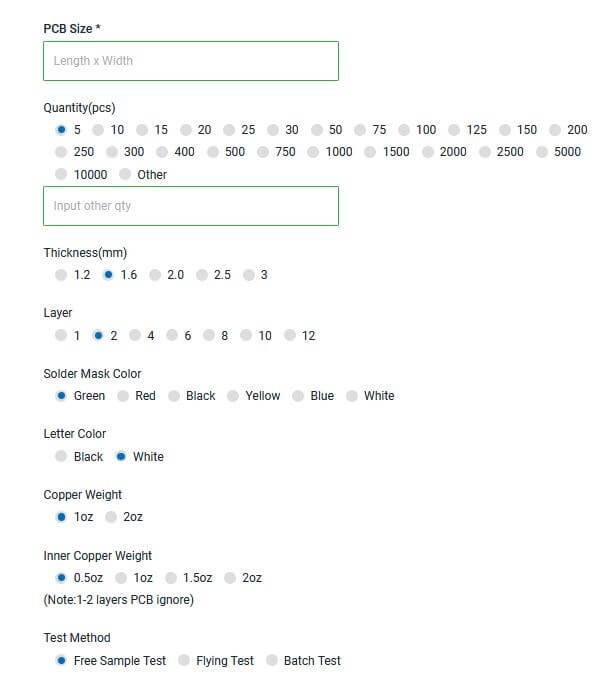
At present, the PCB industry has a number of sampling vendors, OLINAPCB not only stable and reliable quality but also very fast delivery, with 1-2 layers of the fastest 12 hours, 4 layers of the fastest 24 hours, 6-14 layers of the fastest 48 hours delivery.
4. Sample board inspection and function test
After receiving the boards, the sample boards are fully functionally verified to ensure that they meet the design requirements:
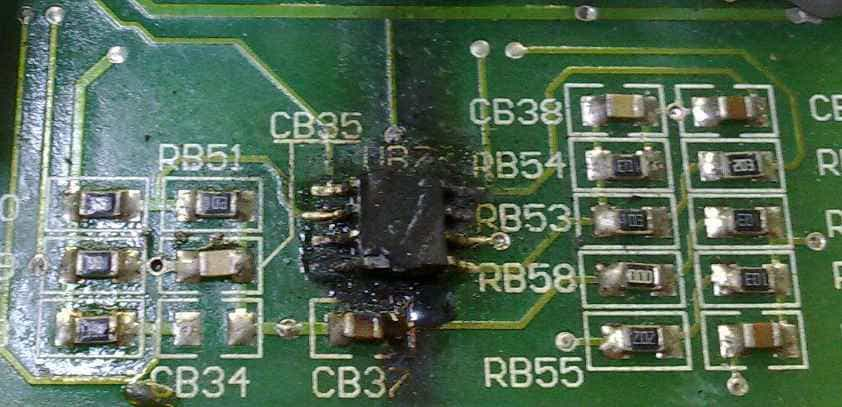
- Appearance check
Check whether the board surface is flat, with no warping or deformation
Check whether the pads and holes are clean and whether the solder mask is covered completely. - Electrical performance test
Verify the circuit’s on-off and impedance characteristics with specialized test equipment.
Conduct signal integrity tests on high-frequency circuits to ensure that there is no signal loss or distortion. - Functional verification
Assemble components and run actual functional tests to ensure that the PCB meets design requirements.

