Because the manufacturing process of printed circuit board is complex and the process is cumbersome, there are many quality defects in its manufacturing process, which seriously affects the quality of the final product. In order to reduce the unqualified rate of PCB and effectively control the quality defects in the production process, the main quality defects in the main manufacturing processes of PCB are briefly analyzed, so as to provide the necessary theoretical basis for solving the defects in the actual production. Following we will discuss the porous metallization and etching process.
Analysis of Main Defects in Porous Metallization Process
Electroplating Cavity
Refers to the hole like area exposing the substrate in the metal layer deposited on the metallized hole wall.
Causes of electroplating cavity
- The cleaning treatment of the hole wall before metallization is not good. During activation treatment, there are attached particles and bubbles on the hole wall, so that there is no activation, so that the chemical copper precipitation can not be carried out, resulting in the cavity of the final product.
- When electroplating tin lead alloy on the pattern, local attachments and bubbles are on the hole wall. During etching, the copper in the part not plated with tin lead is corroded to form a cavity.
Tumor
Refers to the metal tumor like protrusion formed on the surface of the hole wall during electroplating (as shown in Figure 3).
Causes of tumours
- The wall of the drilled hole is extremely unsmooth, with serious glass fiber protrusion.
- Particles in the plating solution are plated and coated in the coating, or the current density is too high.
- The proportion of additives for bright copper plating is out of balance.


Crack or Corner Crack
This crack refers to the crack that can be observed under the microscopic effect of less than 200 times after baking the tested test plate at 120 ℃ for 4 hours and floating dipping solder at 288 ℃ for 10 seconds. It is worth noting that it should not be checked for cracks at a magnification higher than 200(Show as Figure 4). Since the bonding part between the coating and the bottom layer always changes during sample preparation, it is unreasonable to consider the normal bonding gap as electroplating cracks.
It is very important to judge whether it is true coating crack and corner crack, because this crack eventually leads to circuit failure and affects the reliability of the whole board.
Causes of hole metallization crack or corner crack
When the printed board is heated, the expansion coefficient of the epoxy glass cloth below the glass transition temperature (TG ≈ 120 ~ 140 ℃) in the Z direction is 6 ~ 9 × 10 – 5, when the temperature is above Tg, the expansion coefficient is 2.5 × 10 – 4, while the copper expansion coefficient is 1.7 at 20 ℃ × 10 – 5, 1.8 at 230 ° C × 10 – 5。 It can be seen that when the printed circuit board and components are assembled and the thermal shock is carried out at 265 ℃, the expansion coefficients of the two materials are different, resulting in different forces acting on the metallization hole, especially at the corner of the metallization hole. When the toughness of the copper coating cannot meet the requirements of stress and deformation, cracking will occur. In order to overcome this defect, in addition to materials, the quality of point copper coating must be strictly controlled.
Analysis of Main Defects in Etching Process
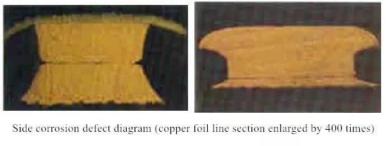
Side Corrosion
A groove formed on the side of the conductor due to etching, and the degree of side corrosion is described by the depth of the groove (as shown in Fig. 5). After causing side corrosion, the pad size will change and the conductor will become very thin. For ordinary printed board, the amount of side corrosion of conductor should not exceed the total thickness of metal, and the side corrosion of precision thin wire strip should be strictly controlled. Lateral erosion is inevitable at all times. We can only try to reduce it, but we can’t eliminate it.
Causes of large amount of side corrosion
- The thickness of copper foil is too large.
- The etching solution is not etching in the best working state.
- Extended etching time.
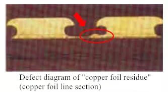
Copper Foil Residue
The so-called copper foil residue refers to the copper foil residue caused by insufficient etching at the root of the copper foil of the formed line (as shown in Figure 6).
Causes of “copper foil residue”
- During the manufacturing of electroplated copper foil, ed copper foil is rapidly plated with a high current density of 1000asf, and grows rapidly upward with columnar structure. At the beginning, the particles are fine, at the end, the particles of the rough edge line are large, and there are additional copper nodules and heat-resistant brass layer added by rough post-treatment. In addition, when pressed at high temperature, its edge lines step into the resin, so it is not easy to completely etch through.
- The upward board surface will have pool (inner layer) or ditch (outer layer) effect. In addition, one copper and two copper are plated too thick. Under the joint attack with the eaves effect of tin lead layer, the board edges and corners are dense in the circuit area, which often leads to incomplete etching.