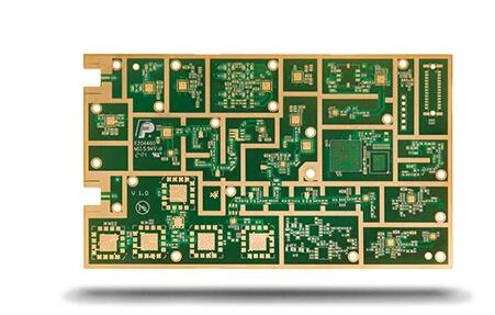
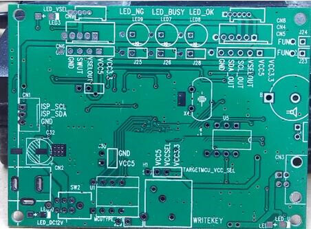
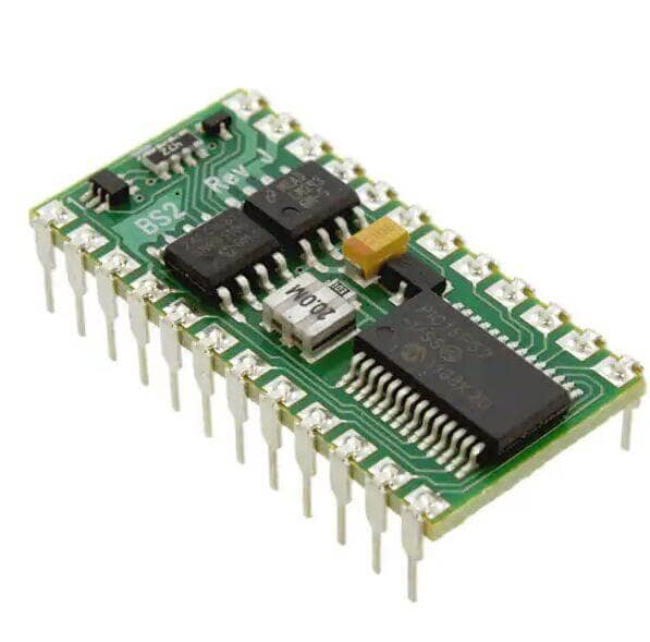
Today, radio frequency circuits are used in various electronic products, including medical, industrial control, and communication products.
What is an RF Circuit Board?
The frequency range of radio frequency is usually 300Khz-300Ghz. The signal above 300Khz is radio frequency, and the signal above 300Mhz is microwave. There is a considerable difference between radio frequency and microwave circuits and typical digital circuits and analog circuits. RF signals are essentially very high-frequency analog signals and therefore, unlike digital signals, at any point in time, RF signals can be at any voltage and current level between the minimum and maximum limits. In addition, the signal in a single band can be narrow or wide and travel on a carrier with a high frequency.
In conclusion, RF circuits face different challenges in PCB design than high-speed digital signal circuits.
Design Challenges of RF Circuits
When dealing with RF circuits, PCB design engineers face the following 4 challenges:
- RF circuits are very sensitive to noise, causing ringing and reflections, and must be handled with care;
- Impedance matching is critical in RF circuits. The higher the frequency, the smaller the error allowed. When the total length of the trace from the transmitting end to the receiving end is greater than 1/16 of the signal wavelength, the impedance control of the trace is required (1/16 of the signal wavelength is the critical length of the signal). For example, if you are dealing with a 1Ghz signal and its total length is greater than 375mil, you need impedance control on the traces.
- Return loss must be minimal. At very high microwave frequencies, the echo signal must take the least inductance path. So, without proper PCB design, the echoed signal goes through the power plane, other layers, or some other line, and the impedance of the signal is no longer a controlled state.
- Crosstalk is an important topic in high-frequency designs because crosstalk is directly proportional to the edge rate of the active line. In this case, the coupling energy of the main line will be superimposed on the disturbed line, and the crosstalk problem will become more serious when the board density increases.

RF PCB Design Solutions
Noise
Properly terminating the signal can solve reflection or ringing problems. Another way is to optimize the return path by using an effective ground plane.
Impedance matching
The PCB designer needs to keep the impedance at 50 ohms: 50 ohms at the transmitting end, 50 ohms during transmission, and 50 ohms at the receiving end.
Return Loss
The ground plane below the signal is suitable for providing an echo path. Good continuity of the ground plane under the signal from the transmitter to the receiver minimizes ground loop currents but also helps reduce RF leakage into circuit components.
Crosstalk
Be sure to allow enough space around the signal traces. Keep all the lines entering and leaving the transceiver module as short as possible, and the wiring distance from the high-speed signal should be as far as possible. The distance between these lines parallel to each other should also be kept to a minimum. All of the above measures will reduce the proximity of two wires and the distance between two wires running in parallel, thereby reducing crosstalk.
Other solutions include reducing the dielectric spacing between the line and its reference plane or introducing a coplanar structure. Inserting a ground plane between lines also reduces crosstalk by up to 50%.
Avoid loss
In addition to the above factors, there are other signal losses. The first is the skin effect loss of the signal, especially on the signal lines. Dielectric loss is closely related to the skin effect, both generated when extremely high-frequency electrons pass through a conductor. For example, they bounce back and forth with the electrons on the FR4 PCB substrate. During this interaction, some of the energy of the electrons passing through the conductor is transferred to the electrons of FR4, thus, the signal energy is converted into heat, which is subsequently lost, and a dielectric loss occurs.
In this case, it is best to use polytetrafluoroethylene for extremely high-frequency microwave circuits, known in the industry as PTFE. This type of laminate has a dissipation factor of about 0.001 (FR4 has a dissipation factor of 0.02).
Laminate properties
When dealing with RF circuits, designers need to consider laminate properties such as dissipation factor and dielectric constant and their variations. FR4 has a higher dissipation factor than high-frequency laminates such as Rogers and Nelco, which means that when using FR4, high insertion loss occurs.
These losses are also frequency dependent and increase with frequency. Second, the Dk value of FR4 can vary by as much as 10%, which in turn changes the impedance. High-frequency plates have more stable frequency characteristics. Then there is the Dk value itself. For microwave circuits, the Dk value is related to the size of the circuit components, so the designer can reduce the size of the circuit by choosing a laminate with a higher Dk value.
RF Circuit Design Tips
To achieve a more reasonable layout and better anti-interference ability of RF PCB, PCB design engineers should master the following design skills:
- Using the inner layer as the power ground layer can play a role in shielding and reducing stray inductance. Shorten the length of the signal line to reduce cross-interference between signals.
- The corner of the circuit wiring must be 45°, which will help reduce high-frequency signal emission and coupling between each other.
- The shorter the circuit layout length, the better.
- The fewer vias the better.
- The layout between layers should be vertical, the top layer should be laid out horizontally, and the bottom layer should be laid out vertically, which will help reduce signal interference.
- Increase ground layer copper to reduce signal interference.
- Doing shielding cover treatment on the key signal wiring can significantly improve the anti-interference ability of the signal. Of course, the interference source can also be treated with a shield to avoid interference with other signals.
- Signal routing should avoid loops, and following the daisy chain layout is recommended.
- In the power section of the IC, bridge decoupling capacitors.


