PCB Stack Design
Stacking Mode
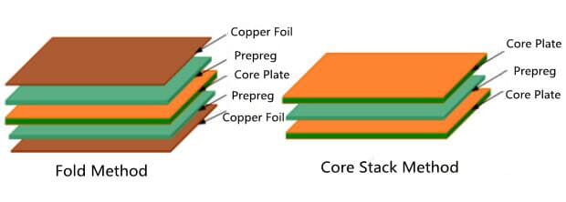
- The recommended stacking method of PCB is foil stacking.(show as Figure 1)
Note:
There are two kinds of PCB stacking design: one is the structure of copper foil with core, which is called foil stacking for short; The other is the core stack method. The core lamination method can be used for special material multi-layer plate and plate mixed pressing.
- The outer layer of PCB generally uses 0.5oz copper foil, and the inner layer generally uses 1oz copper foil; Try to avoid using the core board with different thickness of copper foil on both sides in the inner layer.
- PCB stack method adopts symmetrical design.(show as Figure 2)
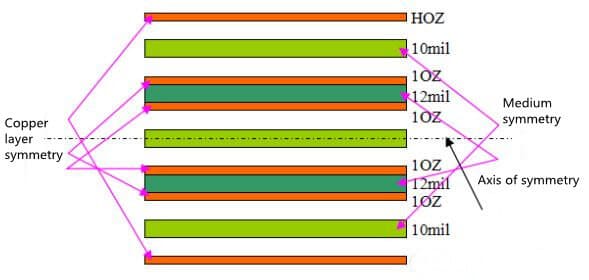
Symmetrical design means that the thickness of insulation layer, semi cured sheet type, copper foil thickness and pattern distribution type (large copper foil layer and circuit layer) should be symmetrical relative to the vertical center line of PCB as far as possible.
General Principles of PCB Size Design
Machinable PCB size range
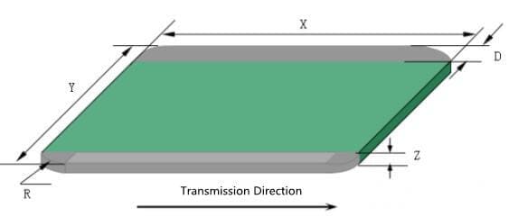
The size range is shown in Table 1 & Figure 3
Table 1: PCB size requirements
Single side mount | Single side mixed | Double side mount | Conventional wave soldering double side mixed loading | |
Length(X) | 51.0 -508.0 | 51.0 -490.0 | 51.0 -508.0 | 51.0 -490.0 |
Width(Y) | 51.0-457.0 | 51.0 -457.0 | 51.0-457.0 | 51.0-457.0 |
Thickness(Z) | 1.0-4.5 | 1.0-4.5 | 1.0-4.5 | 1.0-4.5 |
PCBA weight (reflow soldering) | ≤2.72kg | ≤2.72kg | ≤2.72kg | ≤2.72kg |
Chamfering(R) | ≥3(120mil) | ≥3(120mil) | ≥3(120mil) | ≥3(120mil) |
PCBA weight (wave soldering) |
| ≤5.0kg |
| ≤5.0kg |
Width of the transfer edge device and welding point no distribution area(D) | 5.0 | 5.0 | 5.0 | 5.0 |
The width thickness ratio of PCB requires Y / Z ≤ 150.
The length width ratio of veneer should be x / Y ≤ 2.
The thickness of the plate is less than 0.8mm, and the copper foil of each layer of Gerber is evenly distributed to prevent plate bending. There are a lot of small plates, so it is recommended to use the fixture for SMT.
If the size of the unit board can not meet the above requirements in the size of the forbidden area of the device on the transmission side, it is suggested to add an auxiliary side with a width ( ≥ 5mm) to the corresponding board side.
In addition to the special needs of structural parts, the device body shall not exceed the PCB edge, and shall meet the following requirements:
- The distance between the edge of the l-pin pad (or the device body) and the transmission edge is more than or equal to 5mm.
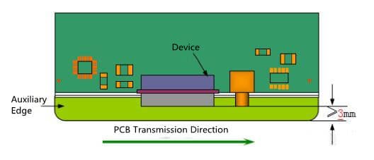
- When a device (non reflow soldering device) extends out of the PCB on one side of the transfer side, the width requirement of the auxiliary side is shown in Figure 4.
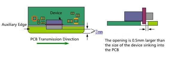
- When a device (non reflow soldering device) extends out of the PCB on one side of the transfer side, and the device needs to sink into the PCB, the width requirements of the auxiliary side are shown in Figure 5.
