Before leaving the manufacturer, the bare PCB (printed circuit board) and PCB assembly (PCBA) must pass the electrical test to ensure that the circuit board has high performance and high reliability in the final product. Conduct electrical tests to find electrical and circuit problems, such as short circuits, open circuits, resistance, capacitance, etc. All these indicate whether the bare or assembled plate is manufactured correctly.
At first, the flying probe test is only suitable for bare board testing, and it has been effectively applied to the online test simulation of bare board and assembly board. The appearance of the flying probe test has changed the test method of low capacity and fast rotating assembled products. By testing the circuit board with flying needles, the product design cycle will be greatly shortened and the time to market will be shortened thereafter.
What is a flying probe test?
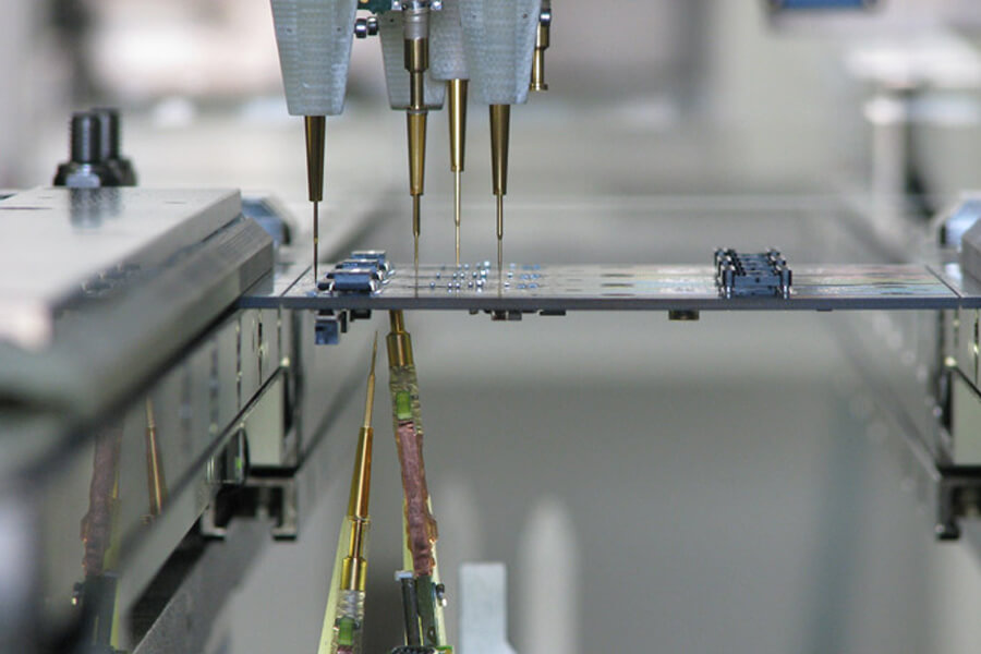
In fact, the flying probe test can be used as an upgrade of the flying probe test. The flying probe tester uses the probe to replace the nail bed. The flying probe tester is equipped with four connectors along the XY axis and can move at high speed.
When the flying probe tester works, the unit to be tested (UUT) will first be transmitted to the internal tester through the conveyor belt or other UUT. Then, the probe will contact the test pad and through-hole, so that the defects of UUT can be found. The probe is connected with the driver (such as signal generator, power supply, etc.) through a multiplexing system and sensors (such as digital multimeter, frequency counter, etc.), through which the components belonging to UUT can be tested. When a component is being tested, other components on the same UUT will be shielded from the test and stop reading interference.
The flying probe tester can test short circuits, open circuits, and component values. In addition, the flying probe tester is equipped with a camera to help find the missing components and check the polarity of the components. Because the positioning accuracy and repeatability of the probe reach 5 μ M to 15 μ M, the flying probe tester can accurately test the manufacturing of UUT.
Comparison between nail bed test and flying probe test
Compared with the nail bed tester, the flying probe tester performs better and more effectively in PCB assembly tests. First, the test development cycle will be reduced so that the final product can enter the market at a higher speed. Secondly, the application of a flying probe tester will reduce the cost and no longer need the fixture for the nail bed test. Third, flying probe tests can realize low-capacity tests at low cost. Finally, the flying probe tester can quickly test the assembly prototype.
How does the flying probe tester work?
The flying probe tester can be programmed easier and faster than the traditional ICT (on-line test) system, such as the flying probe test.
To realize flying probe test programming, testers should first convert the data provided by CAD (Computer-Aided Design) engineers into applicable files. Then, the newly generated file will be run through the test program, which contains the new file in the corresponding format. Finally, all files will be created according to UUT’s test requirements and requirements.
Once the test programming is completed, the real flying probe test is in front of you. The test items shall be determined first, such as short circuits. Then, the reference point data conforming to UUT shall be extracted from the CAD data. Once the UUT is fixed on the platform, programming will be performed to check for manufacturing or assembly problems.
It is necessary to point out that the commissioning should be completed before the official test. In addition, compared with the conventional ICT test, the debugging of the flying probe test can be completed in a shorter time.
Advantages of flying probe test
According to the above definition and working principle, the flying probe test has the following advantages:
- Short test development cycle;
- Relatively low test cost;
- High conversion flexibility;
- Provide rapid feedback to PCB design engineers during the prototype design phase.
Therefore, compared with traditional ICT, the flying probe tests require to shorten the overall test time. In PCB assembly, manufacturing can be started within a few hours after the arrival of CAD files. Therefore, prototype PCB components can be tested several hours after assembly, which is very different from traditional ICT. Traditional ICT usually takes only a few months to test. In addition, due to the low difficulty of setting, programming, and testing, ordinary technicians can operate.
Disadvantages of flying probe test
Every coin has two sides. In addition to the obvious advantages, the flying probe test also has some disadvantages.
Because flying pins have direct physical contact with through holes and test pads, and are prone to small pits on the surface of the circuit board, some OEMs regard them as manufacturing defects. However, nowadays, with the continuous progress of science and technology, this will be overcome by the emergence of upgraded flying probe testers.
Sometimes, when the flying probe tester is dealing with components without test pads, it may contact the probe with the component lead, resulting in poor welding lead or loose lead.
Despite the above shortcomings, the flying pin test is still regarded as an important test method for PCB manufacturing and PCB assembly, and will always play a key role in leading electronic products to achieve excellent performance and high reliability.

