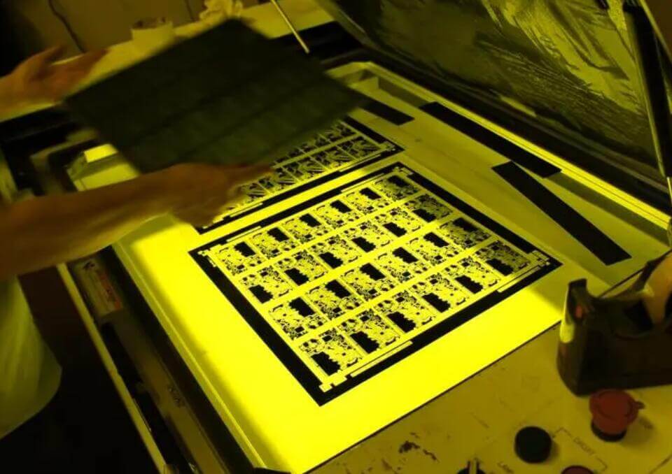
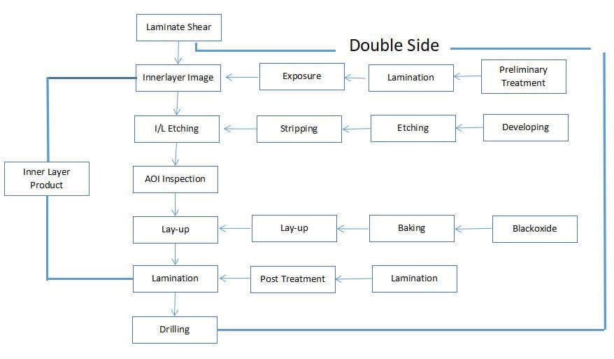
PCB circuit board exposure includes circuit exposure and solder resist exposure. The function is to solidify the irradiated local area through ultraviolet irradiation, and then develop it to form circuit pattern or solder resist pattern.
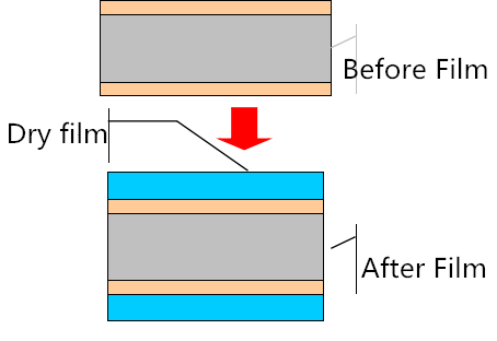
The process of line exposure is to paste the photosensitive film on the copper clad laminate first, and then expose it together with the line graphic negative with ultraviolet light. The photosensitive film irradiated by ultraviolet light will undergo polymerization reaction. The photosensitive film here can resist the scouring of Na2CO3 weak alkali solution during development, and the non light sensitive part will be washed away during development. In this way, the circuit pattern on the negative is successfully transferred to the copper clad laminate.
The process of solder resist exposure is the same. Apply photosensitive paint on the circuit board, and then cover the place to be welded during exposure, so that the pad is exposed after development.
Exposure
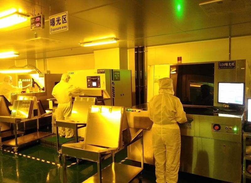
Exposure means that under UV irradiation, the photoinitiator absorbs light energy and decomposes into free radicals, which then lead to the polymerization and crosslinking reaction of luminescent polymerized monomers. After the reaction, a large molecular structure insoluble in dilute alkali solution is formed. Exposure is generally carried out in the automatic double-sided exposure machine. Now the exposure machine can be divided into air-cooled and water-cooled according to the cooling mode of the light source.
Factors affecting exposure imaging quality
In addition to the performance of dry film photoresist, the selection of light source, the control of exposure time (exposure) and the quality of photographic plate are all important factors affecting the exposure imaging quality.
1. Selection of light source
Any kind of dry film has its own unique spectral absorption curve, and any kind of light source also has its own emission spectral curve. If the main spectral absorption peak of a dry film can overlap or mostly overlap with the main spectral emission peak of a light source, the two match well and the exposure effect is the best.
The spectral absorption curve of domestic dry film shows that the spectral absorption region is 310-440nm (nm). From the spectral energy distribution of several light sources, it can be seen that pick lamp, high-pressure mercury lamp and iodine gallium lamp have large relative radiation intensity in the wavelength range of 310-440nm, so they are ideal light sources for dry film exposure. Xenon lamps are not suitable for dry film exposure.
After the type of light source is selected, the light source with high power shall also be considered. Because the light intensity is large, the resolution is high, and the exposure time is short, the degree of thermal deformation of the photographic plate is also small.
2. Control of exposure time (exposure)
In the process of exposure, the photopolymerization of dry film is not “one lead” or “one exposure”, but generally goes through three stages.
Due to the obstruction of oxygen or other harmful impurities in the dry film, it needs to go through an induction process. In this process, the free radical produced by the decomposition of initiator is consumed by oxygen and impurities, and the polymerization of monomer is very little. However, when the induction period is over, the photopolymerization of monomers proceeds quickly, and the viscosity of the adhesive film increases rapidly, close to the degree of mutation. This is the stage of rapid consumption of photosensitive monomers, which accounts for a small proportion of time in the exposure process. When most of the photosensitive monomers are consumed, they enter the monomer depletion region, and the photopolymerization reaction has been completed.
Correct control of exposure time is a very important factor to obtain excellent dry film resist image. When the exposure is insufficient, due to the incomplete polymerization of monomers, during the development process, the glue film swells and softens, the lines are not clear, the color is dim, or even degummed. During the pretreatment or electroplating process, the film warps, infiltrates and even falls off. When the exposure is excessive, it will cause some disadvantages, such as difficult to develop, brittle film, residual glue and so on. More seriously, incorrect exposure will produce deviation of image linewidth. Excessive exposure will make the lines of graphic electroplating thinner and the lines of printing and etching thicker. On the contrary, insufficient exposure will make the lines of graphic electroplating thicker and the lines of printing and etching thinner.
3. Quality of photographic plate
The quality of photographic plate is mainly reflected in optical density and dimensional stability.
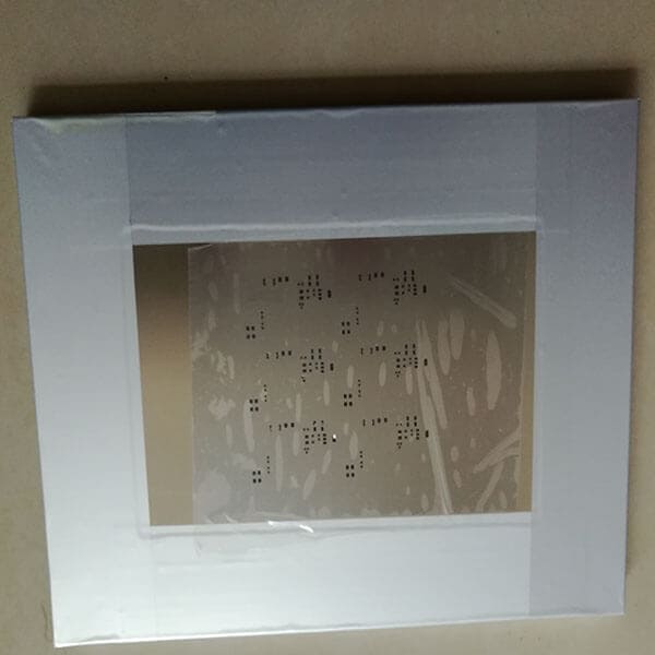
For optical density, the maximum optical density Dmax shall be greater than 4 and the minimum optical density Dmin shall be less than 0.2. The maximum optical density refers to the light blocking lower limit of the surface light blocking film in the left ultraviolet light of the bottom plate, that is, good light blocking can be achieved only when the light blocking density Dmax of the opaque area of the bottom plate exceeds 4. The minimum optical density refers to the upper light blocking limit of the transparent substrate outside the light blocking film of the base plate in ultraviolet light, that is, good light transmission can be achieved when the optical density Dmin of the transparent area of the base plate is less than 0.2. The dimensional stability of the photographic plate (referring to the change with temperature, humidity and storage time) will directly affect the dimensional accuracy and image coincidence of the printed board. Serious expansion or reduction of the size of the photographic plate will make the photographic plate image deviate from the drilling of the printed board. The size of the original domestic so hard film changes greatly due to the influence of temperature and humidity, and its temperature coefficient and humidity coefficient are about (50-60) × 10-6 / ℃ and (50-60) × 10-6 /%. For a S0 plate with a length of about 400mm, the size change of the plate can reach 0.5-1mm in winter and summer. When imaging on the printed board, it may deviate from the distance from half a hole to one hole. Therefore, the production, use and storage of photographic plates are best in a constant temperature and humidity environment.
The dimensional stability of photographic plates can be improved by using thick polyester based silver salt films (e.g. 0.18mm) and diazo films. In addition to the above three main factors, the vacuum system of the exposure machine and the selection of vacuum frame materials will also affect the quality of exposure imaging.

