What is the Thermoelectric Separation Substrate?
The circuit part and the thermal layer part of the substrate are on different circuit layers, and the thermal layer part directly contacts the heat dissipation part of the lamp bead to achieve the best heat dissipation (zero thermal resistance) effect. And the material of the substrate is generally the copper substrate.
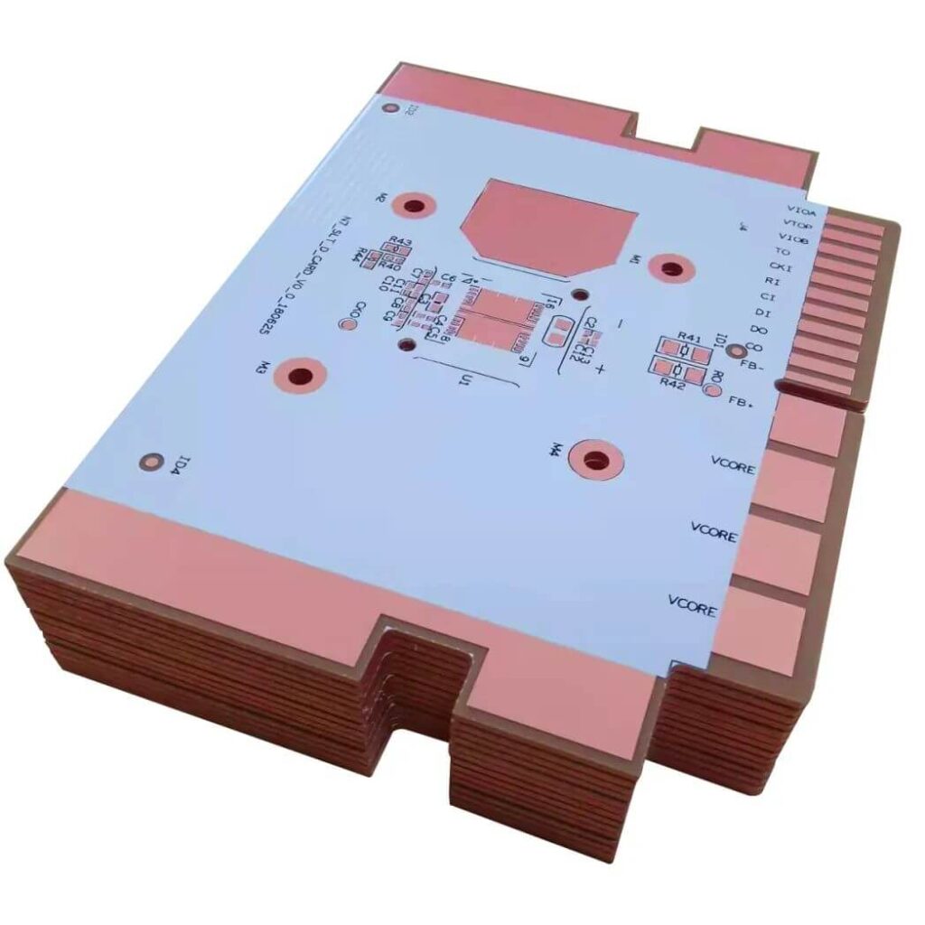
Thermoelectric Separation Substrate Prototype
For low-power lamp beads of about 1W, aluminum substrates are generally sufficient, and copper substrates are not required. Copper substrates are more suitable for high-power products, such as car lights with tens of watts or even hundreds of watts. In order to better meet everyone’s needs, we must come up with higher quality and diversified products.
The thermal conductivity of copper is about 400W, and the “thermoelectric separation” process can better exert the heat dissipation characteristics of copper, so we started prototyping the thermoelectric separation copper substrate.
Difference
What is the difference between thermoelectric separation copper substrate and ordinary aluminum substrate and copper substrate?
For users, the most intuitive difference is the parameters and scope of application:
The thermal conductivity of ordinary aluminum substrate/copper substrate is 1-2W, which is generally single digits, which is more suitable for low-power home appliance LEDs;
The thermal conductivity of the thermoelectrically separated copper substrate is about 400W, which is suitable for high-power, non-ordinary aluminum substrates that can be solved, such as LED lamp beads for automobiles.
Why Power is Different?
Why is the power of thermoelectrically separated copper substrate different from ordinary aluminum substrates and copper substrates?
Thermoelectric separation of copper substrate: The heat dissipation part of the lamp bead is directly connected to the copper substrate, which can achieve the best heat dissipation and heat conduction effect;
Ordinary copper substrate/aluminum substrate: The heat dissipation part of the lamp bead is connected to the aluminum substrate and the copper substrate through an insulating and thermally conductive material. The quality of the thermally conductive material determines the thermal conductivity and cannot exert the heat dissipation advantage of the substrate.
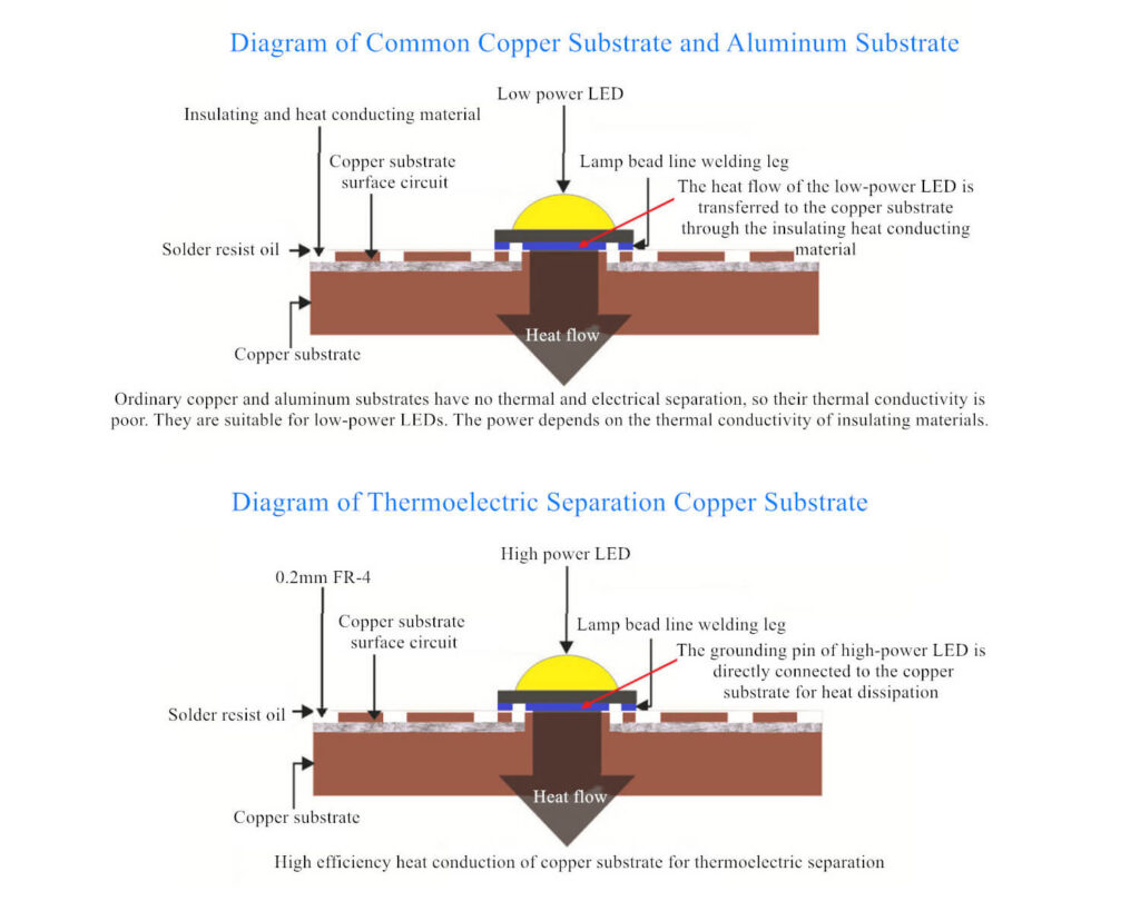
Thermoelectric Separation Process
Why don’t all manufacturers adopt the high specification process of thermoelectric separation?
Thermoelectric separation copper substrate has higher requirements on the production process and technology. Like the production of flexible boards and multi-layer boards, many steps need to be added; while the production of ordinary aluminum substrates and copper substrates is much simpler. The production of FR-4 single panel is similar.
Copper Substrate Thermoelectric Separation Process Technology
Advantages
- Selecting the copper substrate: the density is high, the substrate itself has strong heat carrying capacity, and the heat conduction and heat dissipation are good.
- Adopting the thermoelectric separation structure: contact the lamp bead with zero thermal resistance, reduce the weakness of lamp bead light and extend the life of lamp bead to an extreme.
- The density of the copper substrate is high, and the heat carrying capacity is strong, and the volume is smaller under the same power.
- Suitable for matching single high-power lamp beads, especially COB package, making the lamp to achieve better results.
- According to different needs, various table treatments (immersion gold, OSP, spray tin, silver plating, immersion silver + silver plating) can be carried out, and the surface treatment layer has excellent reliability.
- Different structures can be made according to the different design needs of the lamps (copper bumps, copper concave block, paralleled thermal and
Disadvantages
Not applicable to single crystal chip bare crystal package.
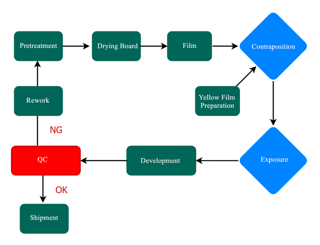
Technological steps of thermoelectric separation of copper substrate
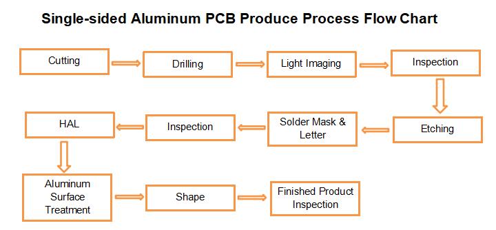
- Cut the copper foil substrate into a size suitable for processing and production.
- Before the substrate is laminated, it is usually necessary to properly roughen the copper foil on the board by brushing, micro-etching and other methods.
- Adhere the dry film photoresist closely with appropriate temperature and pressure. The photoresist will polymerize after being irradiated by ultraviolet rays in the light-transmitting area of the negative film, and the circuit image on the negative film will be transferred to the dry film on the board surface. on the photoresist.
- Tear off the protective film, first use sodium carbonate aqueous solution to develop and remove the unilluminated area on the film surface, and then use the mixed solution of hydrochloric acid and hydrogen peroxide to corrode and remove the exposed copper foil to form a circuit.
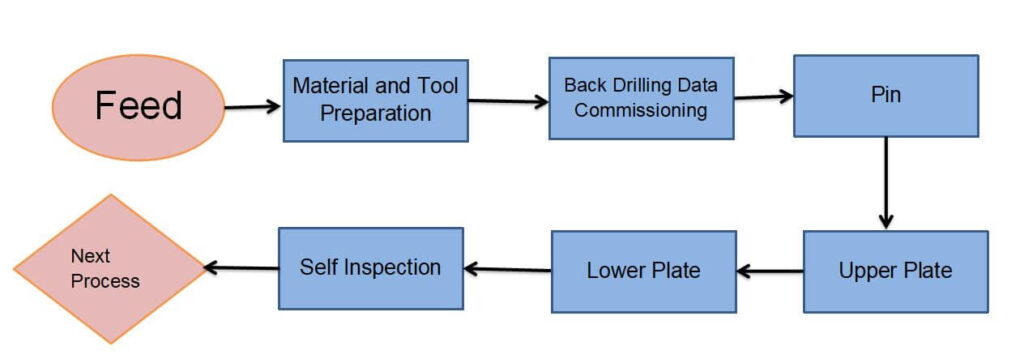
- Wash off the dry film photoresist with aqueous sodium hydroxide solution. For inner-layer circuit boards with more than six layers (inclusive), use an automatic positioning punching machine to punch out the riveting reference holes for the alignment of the interlayer lines.

