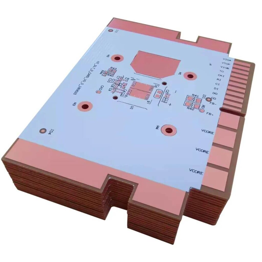
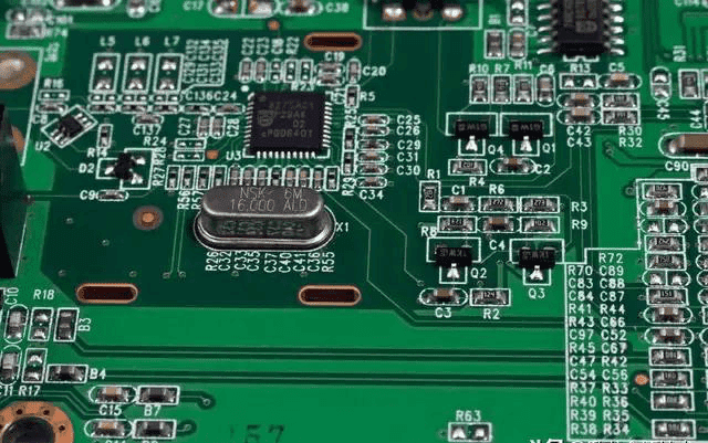
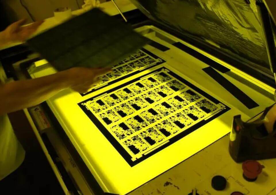
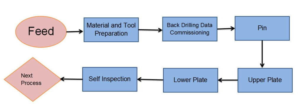
There are many types of metal-based printed boards. Aluminum PCB is one of most used metal PCB. Today we will introduce the produce process of single-sided aluminum PCB.
Single-sided Aluminum PCB Produce Process
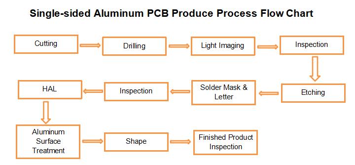
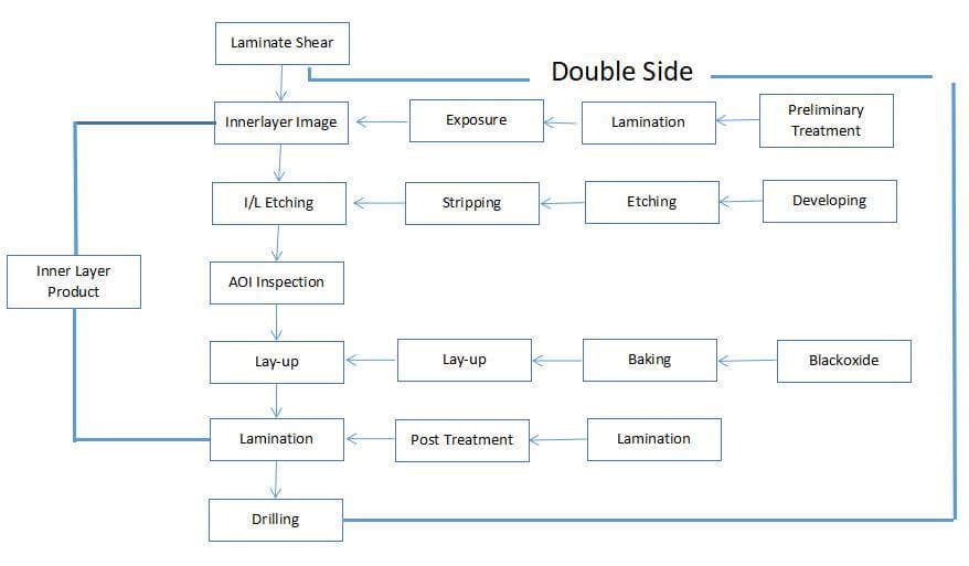
Cutting
Generally, a base material with a protective film on the aluminum surface is used. After cutting, the board does not need to be baked, and pay attention to the protection of the protective film on the aluminum base surface. If PTFE is the filling material, the texture is soft, and it is prone to indentation. It is not possible to open the material with a shearing machine. You can consider using a milling machine to open the material. This can avoid indentation, and can also provide utilization and reduce costs.
Drilling
The parameters are similar to the FR-4 base material, and the aperture requirements are strict. The size of the drill bit should be measured in advance before drilling. The base material with a copper layer thickness of 75um or more should pay attention to controlling the generation of burrs. When drilling, the copper foil is generally upward, and any burrs remaining in the hole will affect the high voltage resistance test. The step-drilling method can be used, and the effect is relatively ideal. The depth of each step of the step-drilling is 0.5~0.8mm, and the height of the lifting tool should be 1mm from the surface of the board. Only the positioning holes are drilled.
Light Imaging
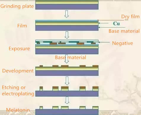
In the surface treatment, only the copper surface is brushed, the aluminum base surface has a protective film, and the film is only attached to the copper foil surface. The exposure and development are the same as the traditional process. If the requirements for the surface of the board are high, mechanical brushing cannot be used for polishing, and only chemical treatment is performed. Note that the integrity of the protective film must be ensured. If there is any damage to the protective film, it must be pasted with glue to ensure the completion of the protective film for the positioning holes. Because aluminum-based panels are not resistant to acids and alkalis.
Etching
Before etching, make sure that the aluminum-based protective film is not damaged. Both acidic and alkaline etching are possible. The process parameters are the same as the traditional process. Pay attention to the compensation of the film. If the copper thickness is ≥75um, attention should be paid to the spot check of line width and spacing to ensure the feasibility of process compensation for line width and spacing during engineering design.
Solder Mask
Use liquid photoimageable solder mask ink. The process is:
Brushing (only for copper surface) → Screen printing solder mask ink (first time) → drying → screen printing solder mask ink (second time) → pre-bake → exposure → developing → post-curing → character printing → turn to the next process.
For aluminum substrates with copper layer thickness ≥75um, you need to do two screen printing inks. The first and second screens are different. Low temperature (75C) pre-baking, post-curing should be performed in stages, for example: 90 C/50min, 110 C/50min, 150 C/60min), air bubbles should be strictly controlled during screen printing.
Hot Air Leveling
If the protective film on the aluminum base is not resistant to high temperatures, the protective film should be removed before the hot air leveling, and the plate should be baked for 130 c/30min before the hot air leveling.
Difficulty of Processing Aluminum Substrate of Metal PCB
- The material is brittle, the resin contains 60~80% filler, and the wire tension is slightly smaller than FR4.
2. The drill bit wears a lot. - Pressing conditions: heating 1.5~2.5 C/min, curing 165 Cx90 min.
- The shape of the tablet will produce white edges.
- When gongs are processed, the aluminum has a larger edge, and special gong knives and V-cut knives are used.
- Hi-pot test for general customers>3000v.

