The PCB industry first developed in the 20th century and continues to evolve. PCBs have made great contributions to the development of the electronics industry. For example, it has led to the emergence and development of small electronic components with very high performance, such as resistors.
We’ll discuss printed circuit boards, their uses, and the step-by-step process of making them. Plus, it will help you learn and find the right PCB for your needs!
1. What is a printed circuit?
Printed circuits are the basis of many electronic devices. These PCBs are the mounting surface for other basic equipment, whether simple printed or complex circuits.
For example, resistors, capacitors, semiconductors, transistors, and diodes require a PCB to function.
2. Why use a printed circuit board?
PCBs are standard because they have many advantages. These boards are usually compact and lightweight in design; thus used in many modern electrical devices. Also, for very complex systems, a PCB is essential. This is because these boards are easy to use and maintain. Additionally, these boards are cost-effective as they are much less expensive to produce.
Some common markets where you can find PCBs include:
Aerospace
Continuous advancements in aerospace technology require compact but complex circuit boards. Due to the lack of connectors, flex, and rigid-flex circuits have excellent durability and survivability.
Medical
The tiny size of the available PCBs makes using the best medical equipment easier. For example, medical hearing aids use PCB technology.
Primarily, rigid-flex boards are essential when there is a need to reduce device complexity. These boards typically do not require flex cables and connectors that use more space.
Industry and commerce
In both industrial and commercial markets, PCB technology is revolutionary. Boardrooms have transformed everything from manufacturing to supply chain management. Additionally, using these boards makes it easy to use automation to guide devices. This approach reduces labor costs while increasing throughput.
Army
Most military equipment and machinery experience a lot of heavy knocks and knocks. Just like any other market sector, military equipment also integrates PCB technology. These devices require mechanical and electrical performance. For example, flexible and rigid-flex packaging requires modification. Both package types can withstand continuous shock and vibration without damage.
3. What is the PCB made of?
Printed circuit board materials are fiberglass/plastic substrate, solder mask, copper, and named inks.
Plastic substrate/fiberglass
Manufacturers can use flexible or rigid surfaces when fabricating PCBs. These two surfaces completely depend on the PCB design required for the project. Importantly, tough surfaces require polyamide fiberglass or FR4. At the same time, the flexible surface uses flexible materials such as high-temperature polyamide film. Some common non-conductive substrates for flex include polyamides, liquid crystal polymers, polyethylene, and polyester. Additionally, these substrates provide a non-conductive surface on which all conductive circuits run.
Copper
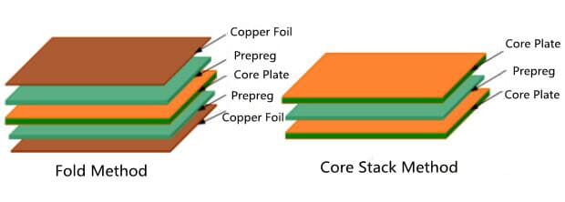
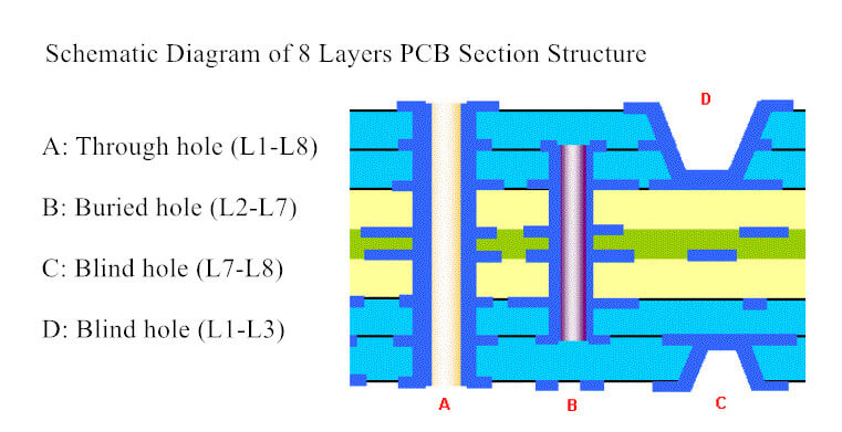
Copper wire has a very high conductivity. The plastic substrate used has thin copper traces laminated on all plastic sides. However, for multilayer PCBs, the structure is different. Multiple layers have alternating layers of copper that act as conductive material for insulating material.
Solder mask
Solder mask is a fluid typically applied to the outer layers of rigid printed circuit boards. Importantly, its job is to cover the copper pieces to keep them from oxidizing. Additionally, when all components are on the board, the fluid is retained and controls the flow of molten solder. When liquid solder flows off the surface, it has the potential to connect two adjacent circuits, creating a short circuit. It is worth noting that the solder mask has a typical green color. However, other colors such as blue, white, red, and transparent can also be used.
After applying the solder mask, the next step is to print barcodes, identification information, and markings. These tags are nomenclature. Crucially, jargon facilitates accurate PCB assembly.
4. The type of printed circuit board.
Rigid PCB
Rigid PCB types consist of a rigid fiberglass substrate. This feature makes PCBs cheap and practical. However, it is not flexible. Unlike flex PCBs, rigid PCBs are less expensive to produce. However, they are less general and thus difficult to adapt to certain device design practices.Flexible PCB
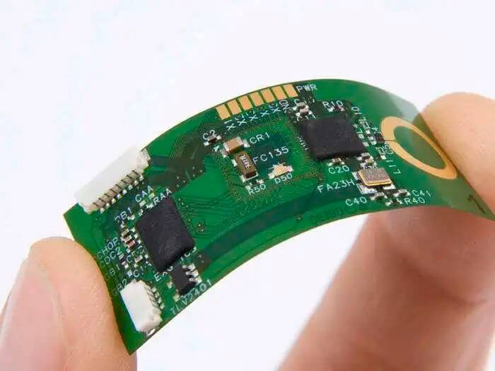
This PCB has an excellent flexible substrate. This feature makes them versatile and can be installed in oddly shaped devices. These boards are adaptable and have no specific shape. Also, unlike rigid PCBs, flexible PCBs have higher heat resistance.Rigid-flex PCB
Rigid-flex PCBs reduce the weight and size of circuit boards by compactly containing the electronic interconnections within the board. This PCB type is also durable, strong, and flexible, combining the notable qualities of rigid and flexible PCBs.5. PCB design factors and processes
PCBs come in many different design types. Importantly, understanding the design process is critical.
- The environment in which the PCB works.
- PCB flexibility.
- PCB assembly and installation.
- The number of configurations and techniques required by the PCB.
- The type of application in which the PCB will operate.
6. How to make PCB step by step?
The following steps can help guide you in developing a suitable PCB.
- The copper layer is chemically imaged and etched with small paths to connect the electronic components.
- The copper layers are laminated with an adhesive material that acts as insulation.
- Holes are plated and drilled on the PCB to electrically connect all copper layers.
- The paths on the outer layers of the board are imaged and plated.
- Cover the board outline with a solder mask, then print naming marks.
- Machine the board according to the dimensions in the perimeter file.
After completing these steps, you can mount the components onto the PCB.

