To restore deleted isolated copper or hollowed-out copper skin in PCB design, the methods vary depending on the software and design context. Here’s a step-by-step guide based on common scenarios and tools:
1. Restoring Isolated Copper (Dynamic Copper)
For Allegro or Similar Tools:
- Re-flood Dynamic Copper: If isolated copper was deleted due to changes in via placement or design rules, re-flood the dynamic copper by:
1. Using the Flood or Hatch command to regenerate the copper pour.
2. Merging shapes: Add a new dynamic copper patch with the same net in the isolated area, then use Merge Shapes to combine it with the existing copper. - Manual Recovery: If the isolated copper was manually deleted, redraw the shape or use the software’s undo function (e.g., Ctrl+Z).
For PADS:
Re-fill Copper: PADS does not save copper data after closing; reopen the file and use Fill (hatch) or Flood to restore copper based on retained outlines.
2. Restoring Hollowed-Out Copper (Cutouts)
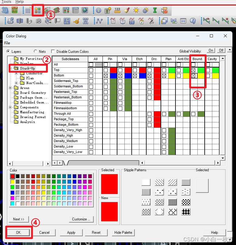
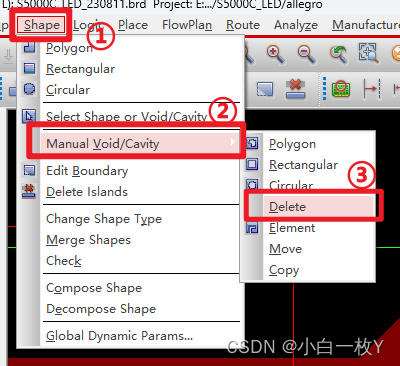
Display and Recover Cut Edges:
Step 1: Enable the display of copper cutout traces (usually in the view settings).
Step 2: Select the cutout boundary and delete it, allowing the copper to automatically refill the hollowed area.
Alternative: Redraw the copper shape if the cutout cannot be directly removed.
Preventing Future Issues:
- Avoid Over-Cutting: Ensure cutouts do not create unintended isolated sections. Use design rule checks (DRC) to flag potential issues.
- Use Solid vs. Grid Copper: Solid copper is less prone to fragmentation but may require thermal reliefs for soldering.
3. General Tips for PCB Copper Management
Dynamic vs. Static Copper: Dynamic copper (e.g., Allegro) updates automatically but may require manual fixes for isolated areas. Static copper is stable but less flexible for edits.
DFM Checks: Before finalizing, verify that no unintended isolated copper or excessive cutouts exist, as these can cause manufacturing defects.
When to Consult Documentation
If the above steps fail, refer to your PCB software’s manual or support forums (e.g., Cadence Allegro
or PADS). For complex cases, CAM engineers may need to adjust Gerber files post-design.
For specific software workflows, tools like Allegro’s IslandDelete or PADS’ Plane Connect may offer additional options.

