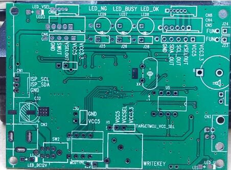
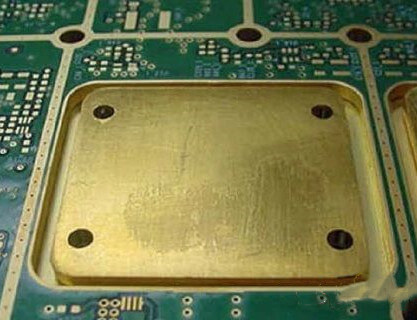
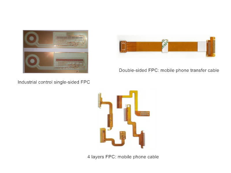
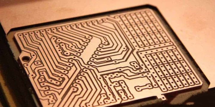
A PCB copper plane is a layer in a PCB with copper on it after etching, usually traces and pads or power and ground planes.
PCB copper material
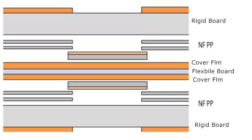
- Copper foil
Copper foil is the cathode portion of the electrolytic material, which is deposited on a continuous thin metal foil layer on the PCB substrate. You can easily bond it from the outside to the insulating layer, which accepts the protective layer and is etched to form your circuit pattern. - Prepreg
Prepreg is picked from prepreg and is known as fiberglass impregnated with resin. This resin is pre-dried, however, it is not hardened. So when heated it sticks, flows, and is completely submerged. Therefore, the prepreg is reinforced with glass fibers via an adhesive layer, just like the FR4 material. Prepreg gets all its names from the fiberglass used.
How thick is the PCB copper layer?
PCB copper thickness is generally divided into 1oz (35µm), 2oz (70µm), and 3oz (105µm). Of course, the thickness of the copper depends on what kind of board you make. The copper thickness of the high current switching power supply is 2oz. Generally speaking, a thickness of 1oz is sufficient for signal transmission.
- The normal double panel is 1 oz.
- The inner layer of a multi-layer board is generally 1/2oz 1/3oz and the outer layer is 1oz 1/2oz 1/3oz.
- The copper thickness of the power board is higher.
70% of the circuit boards use 35µm copper foil thickness, which mainly depends on the purpose of the PCB and the size of the signal voltage and current. In addition, some parts will use 70µm copper thickness for PCBs that require excessive current and 105µm copper thickness.
Also, 12µm is used for ultra-high-density patterns, such as for thin build-up boards, and 105µm for thick, high-current patterns. Thicker copper foil is also used on circuit boards that carry high currents.
When we refer to “thickness,” we’re talking about the weight of copper used in the board. The table below shows a useful conversion table between copper thickness values in mils, microns, and weight.
Copper Weight | Thickness (mil) | Thickness (micron) |
0.5 OZ/square foot | 0.674 | 17.05 |
1.0 OZ/square foot | 1.34 | 34.1 |
2.0 OZ/square foot | 2.68 | 68.1 |
3.0 OZ/square foot | 4.02 | 102.2 |
Although the above table only converts to 3.0 oz/sqft, it can be much heavier. Some manufacturers offer heavy copper weights up to 20 oz/ft² (26.8 mils or 0.34mm PCB copper thickness).
PCB copper layer design
1. Generate output files for copper layers
Use “blink” for pads and avoid “draw/draw” pads when generating output data files. For larger copper areas or copper planes, avoid filling them with small paintings (“painting”). Where possible, use contours or polygons to construct areas or planes. Always include board outlines when exporting copper layers, which helps us identify any data alignment, rotation, or mirroring issues.
2. Non-plated through hole (NPTH)
Remove copper pads from NPTH holes if these pads were not used or not connected to other copper prior to generating the output data file.
3. Copper mesh and copper sheet
Check your final design for small areas of unconnected copper or narrow copper meshes and strips, which can cause production issues.
4. Edge gap of copper plate
For wiring boards:
- Outer layer 0.25mm (10mil)
- Inner layer 0.40mm (16mil)
For boards with score (V-cut):
- Outer and inner layers 0.45mm (18mil)
If you need copper areas or planes to extend to the board’s edge, this must be explicitly indicated in the mechanical layer. Copper should only be used up to the edge of the board if necessary because:
- There is a risk of board edge roughness due to possible tearing of the copper during outline routing (outline).
- Copper creates electrical shorts between layers.
- Copper up to the board’s edge is incompatible with scoring (V-cut).
5. Plate edge plating
Please specify if you need to plate the board’s edge or part of it in the mechanical layer. Additionally, if the board edge is the board, copper must be placed on the top and bottom layers with a minimum width of 0.5mm inwards from the board edge.
This is necessary to allow us to produce round-edge plating so that the metallization is physically strong enough to remain attached to the side of the board.
6. Text placed on the copper layer
Any text placed in a copper layer must comply with the design rules for a given category as defined in our PCB Design Guidelines – Category page. All copper text must be properly legible after etching.
Always view the PCB from top to bottom, through the PCB. Therefore, the text on the top layer of the board should be readable, while the text on the bottom layer should be unreadable or mirrored.
7. Avoid “peelable”
“Strippables” occur during production and are small/narrow pieces of photoresist surrounded by pads, traces, and/or planes. These can “flake” during processing and cause shorts or opens.
8. Edge connector
The surface finish for edge connectors is usually so-called hard gold plated over nickel, which allows repeated mating and unmaking of the connector. To help guide edge connectors into sockets, they need to have a chamfered leading edge. The most typical is the PCB golden finger.
9. Sequence
Always provide the correct layer order for multilayer boards. Layer sequences can be given in various ways:
- Indicates the layer number in the copper image by placing a logical number in each layer (1 for the top layer, 2 for inner 1, 3 for inner 2, etc.)
- Make sure the positions of the numbers do not overlap and are visible through the entire PCB.
- Name each layer file to indicate the order to be used (e.g. Top, Inner 1, Inner 2, Bottom).
- Include a clear composition diagram in your mechanical layer files with the correct order and corresponding data file names including all copper layers, solder masks, legend layers, and additional layers such as peel or carbon layers.
- Include a simple ASCII text file with your data indicating which file will be used for which layer, preferably already in the correct build order (this is the least preferred solution).
Suggestions
Pad
Vias not connected to inner layers suggest the removal of pads from inner layers that do not have connected vias.
Ensure the thermal pad is properly defined and complies with the pattern classification selected for Annular Ring (AR), Track Width (Segment Width), and Clearance.
A good practice is to use a 0.20mm (8mil) gap and a 0.20mm (8mil) thermal segment width.
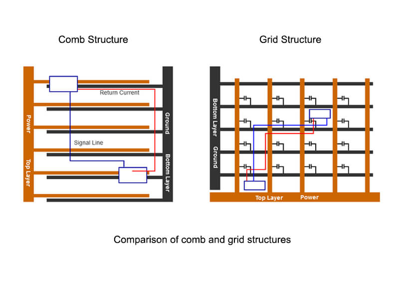
Hatching pattern
Use full copper instead of hatched patterns on copper planes. If you need a hatch pattern, use the following minimum settings:
- Minimum distance or gap between pattern (A) tracks: 0.40mm (16mil)
- Minimum trace width for pattern (B): 0.20mm (8mil)
NOTE: Any hatch pattern that does not meet these minimum requirements will be converted to a full copper plane.
The above is a brief introduction to the PCB copper layer. I hope it can be useful to everyone.

