Routing Design
Line width / line distance and safety requirements for route
The design of line width / line distance is related to copper thickness. The larger the copper thickness, the larger the width / line distance is needed. The recommended line width / line distance for outer layer / inner layer is shown in Table 1.
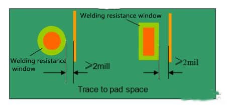
Table 1: Recommended Line Width / Line Spacing
Copper thickness | Outer line width / line distance (mil) | Inner line width / line distance (mil)
|
1OZ | 4/5 | 4/4 |
2OZ | 6/6 | 6/6 |
3OZ | 8/8 | 8/8 |
The distance between outer line and pad is recommended to meet the requirements of Figure 1.
The distance between wiring and board edge is more than 20MIL, the distance between inner power supply / ground and board edge is more than 20MIL, and the distance between grounding bus line and grounding copper foil is also more than 20MIL.
In the area where the metal shell (e.g. heat sink) is in direct contact with PCB, no wiring is allowed. The contact area between the metal shell of the device and the PCB extends outwards by 1.5mm, which is the surface wiring forbidden area.
Outgoing Mode
- Asymmetric routing should be avoided for component routing and pad connection.
- The component should be led out from the center of the end face of the pad.
- When the wire connecting to the pad is wider than the pad, the wire can not cover the pad, and the wire should be led from the end of the pad; When the SMT pad pins with close spacing need to be connected, they should be connected from the outside of the pad, and it is not allowed to connect directly between the pins.
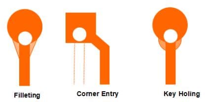
- It is recommended to connect the wiring and the hole in the following way (Figure 2).
Process requirements for copper clad design
- Copper clad design is recommended when the distribution of lines or copper in the same layer is unbalanced or the distribution of copper in different layers is asymmetric.
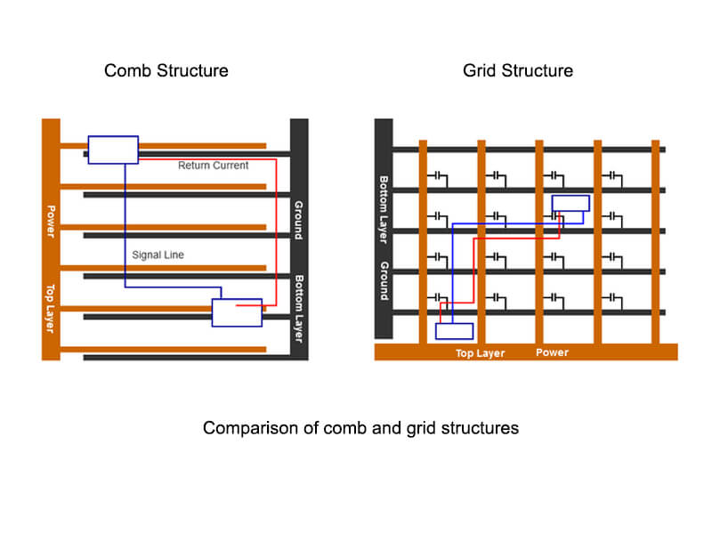
- If there is a large area in the outer layer without wiring and graphics, it is recommended to lay copper grid in this area to make the copper distribution on the whole board surface uniform.
- It is recommended that the size of the space between the copper grids be about 25mil * 25mil.
Screen Printing Design
General requirements for screen printing design
General requirements
- The line width of the screen printing shall be greater than 5MIL, and the height of the screen printing character shall be visible to the naked eye (it is recommended to be greater than 50mil).
- The minimum distance between the screen printing is recommended to be 8mil.
- The screen printing shall not overlap with the pad and reference point, and the distance between the two shall be kept at 6mil.
- White is the default screen printing ink color. If there is special demand, it needs to be explained in PCB drilling picture and text.
- In the design of high density PCB, the screen printing content can be selected according to the needs. The arrangement of silk print strings should follow the principle of the order of the front-up time number from left to right and from bottom to top.
Contents of silk screen printing
The contents of silk screen printing include: “PCB name“, “PCB version“, “component serial number “,” component polarity and direction mark “,” bar code frame “,” installation hole location code “,” component and connector first pin location code “,” plate passing direction mark “,” anti-static mark “,” radiator silk screen printing “, etc.
PCB name and version number:
The board name and version should be placed on the top surface of PCB, and the screen printing of board name and version should be placed horizontally. The font size of the screen printing of the board name should be easy to read. The top surface and bottom surface are required to be marked with “t” and “B” respectively.
Barcode (optional)
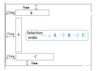
- Direction: the barcode is placed horizontally / vertically on the PCB, and the tilt angle is not recommended;
- Position: refer to figure 3 for the position of the bar code of the standard board; Refer to the position of standard plate bar code for the position of non-standard plate bar code.
Component screen printing
- Components, mounting holes, positioning holes and positioning identification points are corresponding to the silk screen label, and the location is clear and clear.
- Silk screen characters, polarity and direction of silk screen marks can not be covered by components.
- Horizontal device should have screen printing shape at its corresponding position (such as horizontal electrolytic capacitor).
Mounting hole and positioning hole
The location code of mounting hole on PCB is suggested to be “m * *”, and the location code of positioning hole on PCB is suggested to be “p * *”.
Passing direction
PCB with clear requirements for the direction of wave soldering needs to identify the direction of wave soldering. Application: PCB has solder pad, teardrop pad, or device wave soldering direction has specific requirements.
Radiator
The power chip of the radiator needs to be installed. If the radiator projection is larger than the device, the real size of the radiator needs to be drawn by silk screen printing.
Anti static label
The anti-static identification screen printing is preferentially placed on the top surface of PCB.

