For the actual PCB, the best “ground” should be a complete and common ground plane, which can reduce the crosstalk between the wires on the PCB and reduce the electromagnetic interference.
Incomplete Ground Plane
Ground plane segmentation usually occurs on digital analog mixed PCBs. Both the ground plane and the power plane are the same for the return signal. They serve as a reference plane to provide a return path for the return signal. At high frequency, due to the skin effect, the return current always flows under the signal line. However, when a groove appears in the reference plane, the return current bypasses the groove. This bypassed reflux increases the inductance of the whole circuit. The increased inductance can be calculated by the following formula
L=5Dln(D/W) (1)
Where (1): l is inductance, and the unit is NH; D is the trench length, in inches; W is the line width, in inches. This inductance will increase the rise time of the circuit, aggravate the crosstalk between lines, and increase the Q value of the circuit, so that resonance may occur.
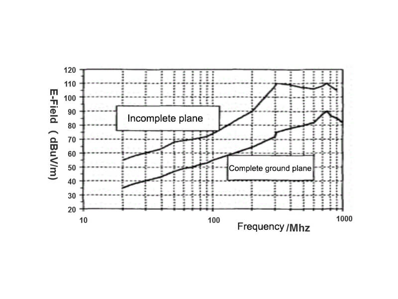
A closed path on the PCB can be equivalent to a current loop antenna. The circumfluence increases the area of the loop and increases the radiation of the loop. The near-field radiation test diagram when a microstrip line has a complete reference plane and an incomplete reference plane is as follows, and the frequency range is 20 MHz ~ 1000 MHz. When the microstrip line crosses the division, its radiation increases by about 20dB.
Reference Plane Division
In actual design, it is unrealistic and economical to completely prohibit plane segmentation. For example, due to the low power consumption of the chip and the complexity of the functions of the single board, there are more than three working power supplies on a PCB. It is inappropriate to arrange one layer of each power supply. Several different power supplies can be arranged on the same plane, and such a layer is divided by different power networks. In order to avoid the interference between different circuits, different circuits set different ground planes. In this way, a layer is divided by different ground planes. For digital analog hybrid circuits, according to the specific situation of single board circuits, three methods can be adopted: segmentation + bridging, zoning but not segmentation.
1) Division: applicable to digital circuit and analog circuit without signal connection
The digital circuit and analog circuit shall be separated during layout, and the device arrangement shall be as compact as possible. During wiring, the signal of digital circuit shall not cross the analog circuit area, the signal of analog circuit shall not cross the digital circuit area, and the signal of analog circuit shall not cross the digital circuit area. The two areas are separated by a sufficient distance. Digital ground and analog ground are separated, and then a single point connection is made at the socket, as shown in the figure below, which can maximally suppress the interference of digital circuit to analog circuit.
2) Split + bridge: the signal lines applicable to the connection between digital circuit and analog circuit are less and concentrated
When two areas have only one connection point, the current cannot flow into another area through one connection point and return from the same point. At this time, the two regions are independent of each other, and the current cannot flow in or out. As shown in the figure below, this form is introduced into analog ground and digital ground. The digital ground and analog ground are divided by grooves, and then the two are connected by bridges. This not only ensures the same voltage between DGND and agnd pins, but also isolates the noise generated by digital circuits. The benefits of using a bridge are similar to a castle with a moat. Only the signal with the right of way can be allowed to pass through. The loop formed on the reference plane through the bridge is the only path allowed to exist.
3) Partition but not division: there are many signal lines applicable to the connection between digital circuit and analog circuit, and it is difficult to concentrate in one piece
The digital circuit and analog circuit shall be partitioned and arranged. During wiring, the signal inside the digital circuit shall not cross the analog circuit area, and the signal inside the analog circuit shall not cross the digital circuit area. The stratum is not divided, but a complete layer to ensure that the signal connected between the two circuits has the smallest signal loop.
4) Bridging of signal circuit: the signal spans at least two plane layers.
When more important signals have to cross the reference plane, the following two bridging methods can be adopted: cross line bridging and capacitance bridging, as shown in below figure.
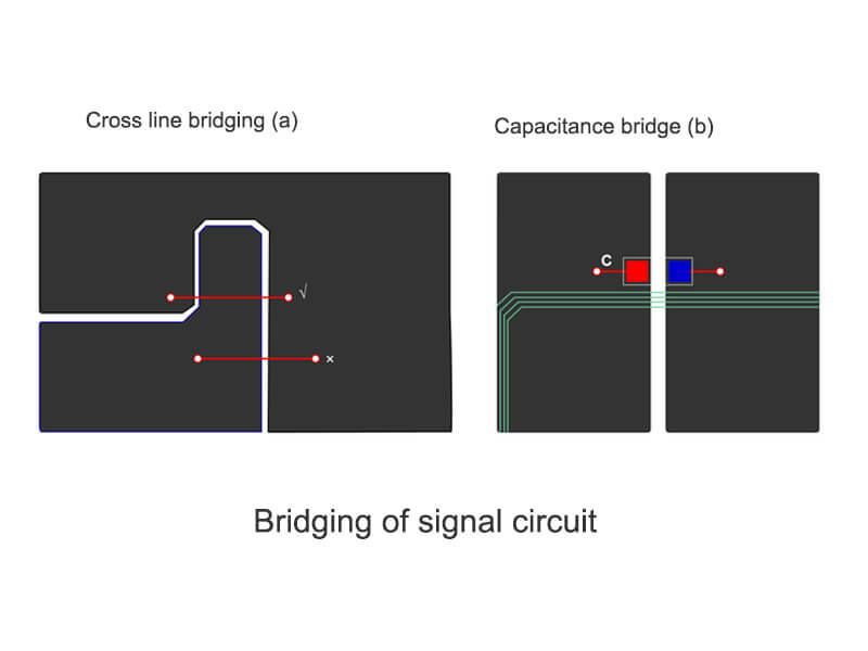
1) Cross line bridging: it is suitable for returning to the original reference plane after signal crossing. The bridge runs on the signal layer, and the route should be as wide as possible. Refer to “cross line bridge (a)” in above figure.
2) Capacitance bridging: when the signal cannot return to the original ground plane after crossing and dividing, one (or more) 0.01uF capacitors can be added at the signal crossing to provide a loop for the signal. Capacitors for this purpose are often vividly called stiching capacitors. The bridge capacitor shall be as close as possible to the signal line to be protected (less than 200mil, better when less than 80mil), and each capacitor shall hold no more than 5 signal lines. As shown in “capacitance bridge (b)” in above figure.
Treatment of Reference Plane
The general treatment principles of reference plane are as follows
- The power plane is close to the ground plane (high frequency circuit only)
When the working frequency of the circuit is very high (e.g. greater than 100MHz), the power plane should be close to the ground plane, which can maximize the capacitive coupling between the power plane and the ground plane and reduce the noise of the power supply. - Multiple ground planes are connected by vias
When there are multiple ground planes in the PCB, the ground planes should be connected together with more scattered vias on the board, especially at the place where the signal is concentrated for layer change, so as to provide a shorter circuit for the signal of layer change and reduce radiation. - When conditions permit, the 20h principle shall be adopted
When implementing the 20h principle, priority should be given to the minimum signal loop and continuous signal impedance. That is, when retracting the power plane, if the adjacent signal layer has routing at the edge of the power plane, the 20h principle can be ignored within this range to ensure that the signal does not cross, and the position of the signal should be derived from the edge of the power plane. - Add ground plane as signal isolation layer
When the number of signal layers is large and the isolation layer needs to be added, the ground plane should be added as the isolation layer instead of the power plane. - Control the extension area of the plane
When designing the power ground plane, the extension area of the plane should be controlled to avoid the overlapping of reference planes of different types of circuits, and there is capacitive coupling between parallel charged planes.

