What’s PCB Prototyping?
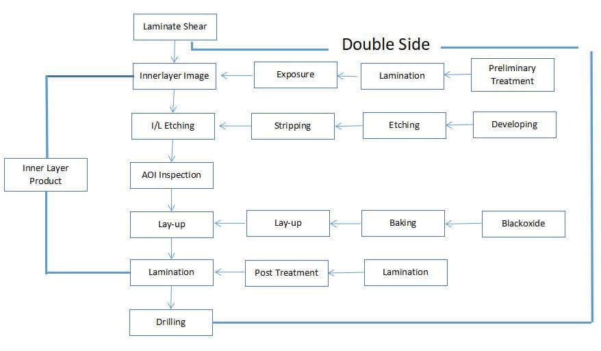
PCB prototype refers to the trial production of printed circuit boards before mass production. It is mainly used in the process of small batch trial production to the circuit board factory after the electronic engineers have designed the circuit and finished drawing PCB.
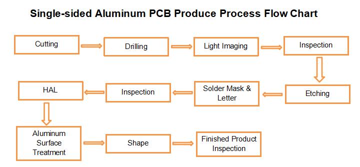
Production Process of PCB Prototyping Manufacturer
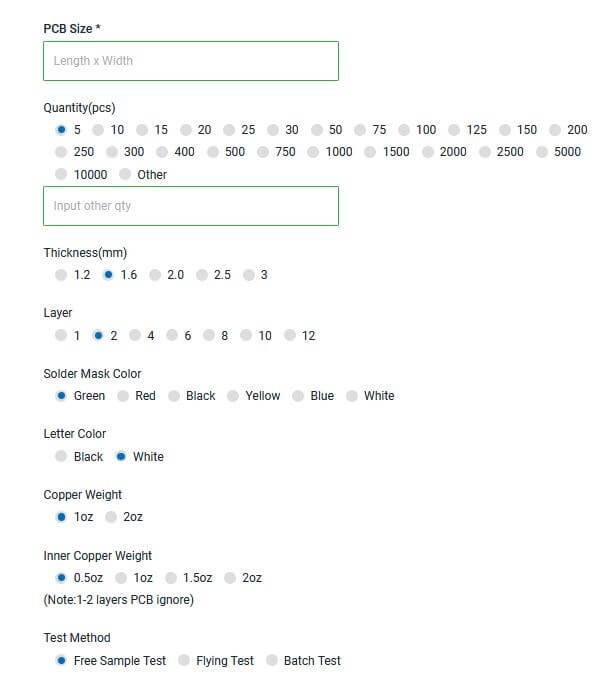
- Contact the manufacturer
First, the company shall inform the manufacturer of documents, process requirements and quantity. - Opening
Objective: according to the requirements of MI, the small pieces of plate are cut into small pieces on the large plates which meet the requirements
Process: large plate → cutting plate according to MI requirements → corner plate → beer fillet / edge grinding → plate out - Drilling
Objective: according to the engineering data, the hole diameter is drilled in the corresponding position on the plate which meets the required size
Process: plate stacking pin → upper plate → drilling → lower plate → inspection / repair - Copper deposit
Objective: copper deposition is a thin layer of copper deposited on the insulation wall by chemical method
Process: rough grinding → hanging plate → automatic copper wire sinking → lower plate → immersion of 1% dilute H2SO4 → thickening copper - Graphic transfer
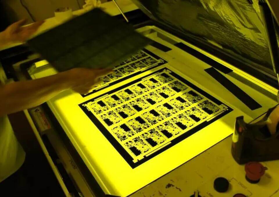
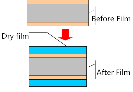
Objective: graphic transfer is the transfer of images on production film to the board
Process: (blue oil process): grinding plate → printing the first side → drying → printing the second side → drying → deflagration → shadow punching → inspection( Dry film process): Hemp board → film pressing → static setting → alignment → exposure → static setting → shadow punching → inspection - Graphic plating
Objective: Graphic plating is to electroplate a copper layer with required thickness and gold nickel or tin layer on the bare copper skin or hole wall of the line
Process: upper plate → oil removal → secondary water washing → micro etching → water washing → pickling → copper plating → water washing → acid immersion → tin plating → water washing → lower plate - Desorbing
Objective: to remove the coating of anti plating with NaOH solution to expose the non – line copper layer
Process: water film: inserting frame → alkali immersion → washing → scrubbing → passing machine; Dry film: plate setting → passing machine - Etching
Objective: etching is to remove copper layer from non – circuit by chemical reaction - Green oil
Objective: green oil is to transfer the green film graphics to the board, and play the role of protecting the circuit and preventing tin on the line when welding parts.
Process: grinding plate, printing sensitive green oil, curium plate, exposure, and shadow drawing; Grinding plate → printing the first side → drying plate → printing the second side → drying plate - Characters
Purpose: character is a kind of mark which is easy to recognize.
Process: green oil after final corner → cooling static setting → network adjustment → character printing → rear corner - Gold Plated
Finger purpose: to coat the plug finger with a layer of nickel / gold layer with required thickness, so as to make it more hardness and wear-resistant process: upper plate → oil removal → water washing twice → micro etching → water washing twice → acid washing → copper plating → water washing → nickel plating → water washing → gold plating.
Tin plate(The purpose of this paper is to spray a layer of lead tin on the exposed copper surface without covering the welding oil to protect the copper surface from corrosion and oxidation, so as to ensure good welding performance. Process: Micro etching → air drying → preheating → rosin coating → solder coating → hot air leveling → air cooling → washing air drying - Forming
Objective: to form the shape required by customers by stamping or CNC gongs, including gongs, beer plates, gongs and hand cutting.
The results show that the accuracy of data Gong and beer board is high, and the lowest tool of manual cutting plate can only do some simple shape。 - Testing
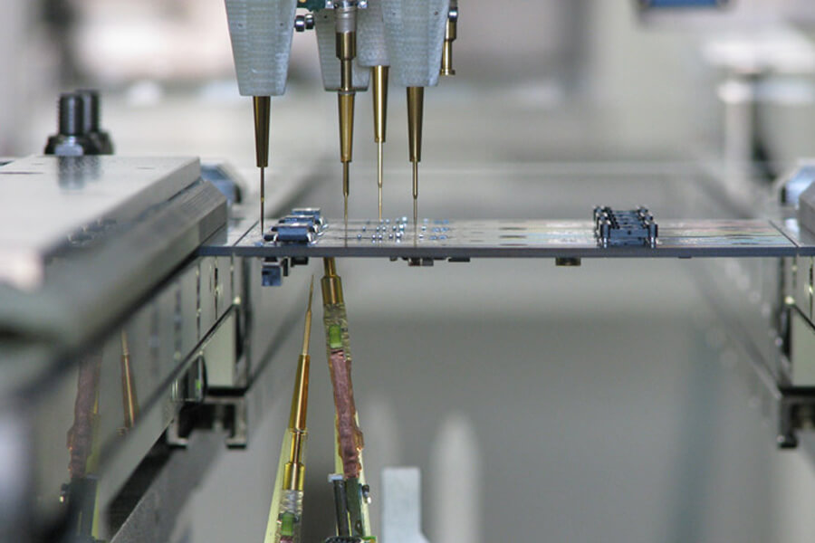
Objective: to detect the open circuit and short circuit which are not easily found by visual inspection through 100% electronic test
Process: upper mold → plate setting → test → qualified → FQC visual inspection → unqualified → repair → return test → OK → rej → scrap - Final inspection
Objective: to check the appearance defects of the board by 100% eye and repair the minor defects to avoid the outflow of the defective parts
Specific workflow: incoming materials → data review → visual inspection → qualified → FQA spot check → qualified → packaging → unqualified → treatment → inspection OK.

