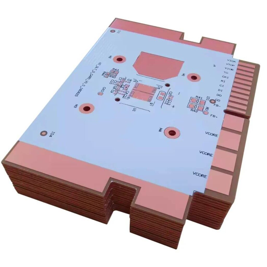
There are a lot of parameters to be confirmed when making PCB. It’s easy to understand the parameters such as size, quantity, plate materials, thickness, solder resist color and silk screen color. But there is some parameters that are not so easy to understand, such as copper thickness, minimum line width / line distance, minimum aperture, through-hole windowing, through-hole cover oil, tin spraying, gold precipitation, and so on.
PCB Prototyping Parameters
Basic Information
Size: Length * Width
Quantity: Depending on the product demand, mass production is more cost-effective. The mini is 5 pieces.
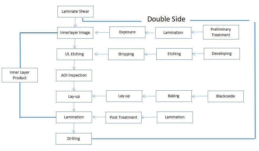
PCB Layers: Double sided board and four layers board are commonly use. We can be used as 20 layers board at most.
Conventional Process
Solder resist color: Generally green
Silkscreen color: Try to have a high contrast with the solder resist color
Plate material: FR-4 common
Plate brand: Shengyi, jiantao, etc
Thickness: Generally 1.6mm
Outer copper thickness: The power is not particularly large, choose 0.5oz
Minimum line width / line spacing: The smaller the difficulty, the higher the difficulty. The upper limit of domestic process is 3 / 3mil.
Minimum hole diameter: 10 / 18mil is recommended for through hole.
Solder mask: Through hole windowing, Through hole cover oil, Through hole plug hole.
Surface treatment: HASL, HASL-LEAD free, Immersion Gold.
Special process: impedance, golden finger, blind buried hole, thick copper plate, multi layer special laminated structure, nickel palladium, special shaped hole, depth control groove, half hole / edging.
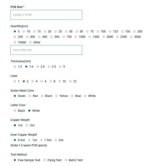
Quantity of boards / board size
The quantity of boards is easy to understand, which is how many boards you want to make. The board size is the size of the board, but the PCB board generally does not have a large size. If necessary, it is often divided into several pieces and then spliced and combined after manufacturing. Of course, PCB boards are generally not too small. If they are too small, there will be some trouble in the production, testing and use of PCB boards, which will lead to the rise of costs.
Board Layers
The number of layers is generally determined during PCB circuit design, so the corresponding number of layers can be directly selected according to the design requirements. Generally speaking, the higher the number of layers, the more difficult the process and the higher the cost. According to the number of layers, PCB can be divided into single panel, double-sided layer and multi-layer board.
Single panel is the most basic PCB. The parts are placed on the same side, while the wires are concentrated on the other side, which is suitable for simple circuits.
Double sided board is widely used. Its top and bottom layers are covered with copper, which can be wired and welded. The middle is an insulating layer, and the circuits on both sides are connected through guide holes. It is suitable for general complex circuits.
The biggest difference between multi-layer board and single panel and double panel is that multi-layer board adds internal power layer and grounding layer, but multi-layer board wiring is mainly based on the top layer and bottom layer, supplemented by the intermediate wiring layer. The number of layers of multi-layer board is generally even (even layers have more advantages than odd layers). However, the number of layers cannot directly explain how many wiring layers there are, because sometimes empty layers are added to control the board thickness. The wiring space of multi-layer board is larger, and the EMC (electromagnetic anti-interference) ability is stronger when the circuit design is reasonable.
Color of solder resist
Green, blue, black, red, yellow and other colors are commonly used. If there are no special requirements, use green. If you use it for your own experiment, you’d better use green, because under normal circumstances, green oil has the best performance.
Silk screen color
White and black are commonly used colors. If the solder resist is green, white characters are generally selected. This is mainly to see clearly. If the color contrast of the heel plate is large, it is OK. If it is white solder resist, black characters should be selected.
Plate Material
Material is one of the important factors affecting the quality of PCB. FR-4 (epoxy resin fiberglass board) is commonly used. It has the advantages of high strength, heat / fire resistance (no combustion), chemical resistance (not easy to corrosion and mold growth), moisture resistance, thermal property (low coefficient of expansion, high coefficient of thermal conductivity), electrical property (non-conductive, insulation) and so on. Therefore, FR-4 has been widely used in the industry.
Plate brand
Domestic common plate brands include Shengyi, Jiantao, Jin’an Guoji, South Asia, Rogers, etc.
Plate thickness
0.8mm,1.0mm,1.2mm,1.6mm,2.0mm…… In fact, there are many commonly used specifications, but if there are no special requirements, it is best to choose the plate thickness of 1.6mm.
Copper thickness
0.5oz,1.0oz,2.0 oz…… In fact, there are many common specifications of copper foil, but if the power is not particularly large, you can choose 0.5oz. If the power is about 100W, you can use 1.0oz. As for the specific selection, there is no unified standard in the industry at present.
Minimum line width / line spacing
Under normal circumstances, the smaller the, the higher the difficulty. At present, the upper limit of process capacity of large domestic manufacturers is mainly 3 / 3mil, and some very excellent ones are about 2 / 2mil.
Minimum aperture
For through holes, it is generally believed in the industry that the minimum is 0.1mm (about 4mil), which is jointly determined by the drilling rig, drilling nozzle and plate; If it is a blind hole, the most advanced laser drill can produce a minimum hole diameter of 25 μ M (about 1mil). In general, the smaller the hole, the more expensive. It is recommended to use 10 / 18mil and 12 / 20MIL through holes, and 16 / 24mil for power holes.
Solder mask
Solder resist covering, or green oil covering, refers to the part of the circuit board to be covered with green oil, which is mainly used for insulation. There are three main types of resistance welding cover: through-hole windowing, through-hole cover oil and through-hole plug hole.
- Through hole window opening, i.e. copper exposure. It refers to that when printing the solder resist layer, windows are opened where there are vias to expose the copper foil (PAD) at both ends of the vias.
- Through hole cover oil means that the solder resist printing plate does not open the window, and the copper foil (PAD) at both ends of the through hole is covered with green oil and cannot be welded.
- Through hole plug hole is to plug the through hole with something so that there will be no hole on the surface. Generally, green oil plug is used, and resin and metal plug are also used.
In fact, there is no requirement for the hole diameter of the resistance welding cover, but no matter which type is selected, the through hole cannot be too large. Generally, the maximum through hole of the plug hole is 0.5mm, and no matter how large it is, it cannot be plugged. Moreover, if the hole is large, it will occupy a large design space and affect the linewidth.
Surface treatment
The brazing point on the circuit board is easy to be oxidized in the air, resulting in poor tin eating or poor contact, which reduces the conductivity of the circuit board. Therefore, the surface treatment of the brazing point is required. Common surface treatment processes for PCB manufacturing include tin spraying, gold deposition, gold plating and OSP. Users can choose the most suitable one according to their own needs.
Tin spraying is a common processing method in the early stage of printed circuit board proofing. It can be divided into lead tin spraying and lead-free tin spraying. After the completion of PCB, the copper surface is completely wetted (the tin is completely covered before soldering), which is suitable for lead-free welding. The technology is mature and the cost is low. It is suitable for visual inspection and electrical testing.
Immersion Gold refers to gold plating on PCB. Gold can effectively block copper metal and air and prevent oxidation. This gold plating process will produce chemical reaction, so it is also called gold plating. The surface of gold deposit is very smooth, the deposition color is very stable, and the ability to resist environmental erosion is strong. Generally, the thickness of gold is 1-3 uinch, which is suitable for SMT, electrical test, switch contact design, aluminum wire bonding and thick plate.
Electroless gold plating, that is, electroless gold plating on PCB, is similar to gold deposition, but higher than gold deposition cost. The main feature is wear resistance. Therefore, electroless gold plating is usually selected where plugging is required.
OSP, or organic solderable protective film, is an organic film grown chemically on the surface of clean bare copper. This film has oxidation resistance, heat shock resistance and moisture resistance. It has flat surface, simple process, easy operation and maintenance, less pollution and low cost. OSP can be said to be the lowest cost in PCB surface treatment process. But the disadvantages are also obvious. First, the protective film is very thin and easy to scratch; Second, the protective film will change color or crack after several high-temperature welding, which will affect the weldability and reliability; Third, it is not acid resistant, and high humidity environment will affect its weldability.
Of course, in addition to the above conventional parameters, making PCB also involves some special processes, including gold finger, impedance, buried blind hole, thick copper plate, multi-layer special laminated structure, special-shaped hole, depth control groove, etc. you can make corresponding design according to the product requirements.

