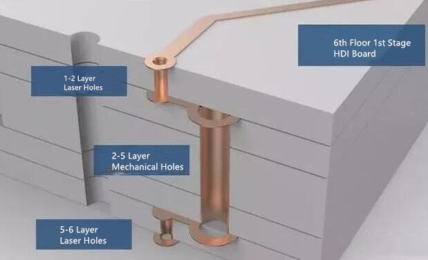
More than 80 years have passed since Paul Eisner officially invented PCB manufacturing technology in 1936, and PCB has developed rapidly and has become an indispensable foundation for the electronics industry. Although the PCB generally only accounts for 5~10% of the cost of the finished circuit board, the reliability of the PCB is far more important than a single component – the component is broken, the circuit board can still be repaired, and the PCB is broken, the circuit board is Can only be scrapped!
When it comes to reliability, this has to bring up the issue of hole metallization in PCBs.
Hole metallization, its core function is to realize the conduction between PCB layers by plating copper on the hole wall. It is the core key point for double-sided and multi-layer boards to function. Therefore, many electronic Giants, such as Apple, Huawei, etc., attach great importance to this.
But in fact, the hole metallization technology is not complicated and can be simply divided into two parts: preparation before electroplating copper and electroplating copper. The quality of electroplating copper depends to a large extent on the preparation before electroplating copper.
Therefore, people in the industry often focus on the PCB reliability issues to the preparation before copper electroplating.
At present, there are three main preparation processes for copper electroplating in the industry: immersion copper, black hole, and black shadow. (There are also colloidal palladium, metal grouting, etc., but they are not the current mainstream and will not be discussed here)
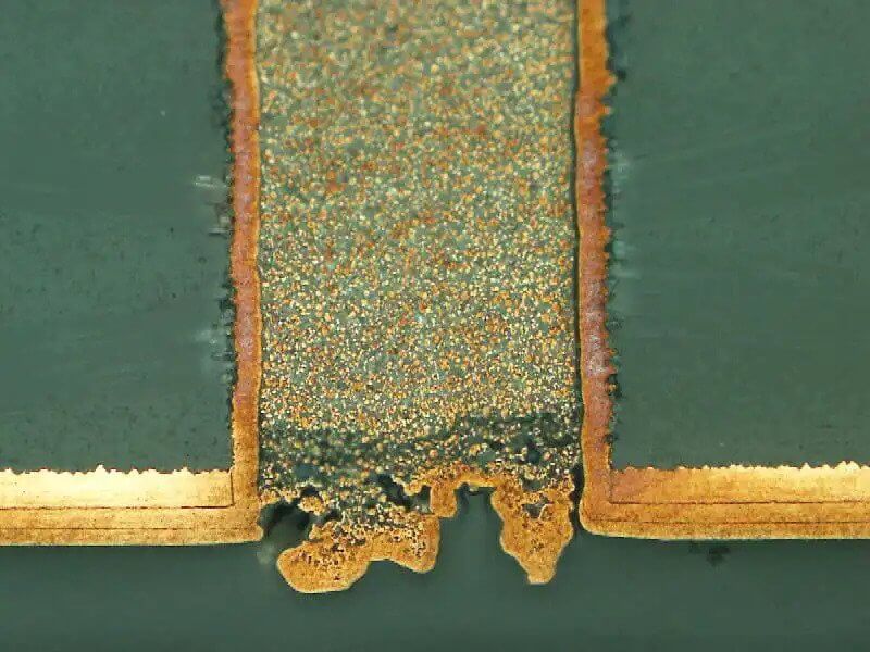
Immersion Copper
Immersion copper, also known as chemical immersion copper, its main principle is to use a chemical substitution reaction to deposit a layer of copper on the hole wall as a conductive lead for subsequent copper electroplating. If it is conventional sinking copper, its thickness is generally about 0.5μm. As the most traditional preparation process for copper electroplating, it has the following advantages and disadvantages.
Advantage
- Metal copper has excellent electrical conductivity (in the wire, copper wire is conventionally used as electrical conductivity);
- The thickness can be adjusted in a wide range and has a wide range of adaptability (currently the lowest in the industry is about 0.3 μm, and the highest can reach 30 μm, which directly replaces the subsequent electroplating copper process);
- The process is mature and stable, and can be applied to all circuit board products (PCB/FPC/RFPCB/carrier board/metal substrate/ceramic substrate, etc.).
Disadvantages
- Contains formaldehyde, which is detrimental to the health of operators;
- The equipment investment is large, the production cost is high, and the environmental pollution is not small;
- The aging control is short, and the general effective time is 3 to 6 hours.
Black Hole
Black hole is a kind of direct electroplating technology. Its main principle is to use physical principles to make carbon powder adsorb on the surface of the hole wall to form a conductive layer, which is used as a conductive lead for subsequent copper electroplating. Typically, its thickness is 0.5~1μm. As one of the current mainstream preparation processes for copper electroplating, it has the following advantages and disadvantages.
Advantage
- It does not contain formaldehyde, which has little impact on the health of workers and less pollution to the environment;
- The equipment investment is not large, the waste treatment is simpler, and the process cost is lower than that of copper sinking;
- The potion and process are relatively reduced, and the timeliness can reach 48H, which is more convenient for maintenance and management.
Disadvantages
- In terms of electrical conductivity, the conductive carbon powder will be weaker than the deposited copper layer;
- Its applicability is not as wide as that of sinking copper. Therefore, although it has been used on a large scale, it is currently mainly used in double-sided panels in the industry, and high-end products such as HDI are hardly used.
Black Shadow
Black shadow, strictly speaking, is a further development of black hole technology. Its principle, advantages and disadvantages are similar, and it is better than black hole. The main difference is that the conductive layer of the black hole is carbon powder, while the conductive layer of the black shadow is graphite.
In addition, black holes are generally not used for high-end products, or with complex processes, but black shadows can be used. The black shadow process has partially replaced copper sinking and is widely used in high-end circuit boards, such as HDI boards, IC carrier boards, etc. Even, sometimes the shadow process is better than the copper immersion process, such as selective pattern plating.
As mentioned above, you may think that the copper immersion process is better than the black hole and shadow process. If you look at it in a general way, the industry generally thinks so, but if it comes to the actual application level, it is not always the case. PCB technology will have its advantages and disadvantages, and then establish its position in practical applications. If it is indeed fully backward, it will naturally be eliminated by the industry.
Therefore, it is considered that the effect of sinking copper > black shadow > black hole can be used as a reference answer, but it cannot be used as a final answer, because it also involves the actual situation of each process using the factory, as well as the equipment used in the process, Potions, parameters, etc.
Therefore, from a real point of view, the process is only a means of making products. As long as the products produced can meet the requirements of shipping, and the manufacturer can also obtain satisfactory profits, then this process can be used.

