Single-sided Printed Circuit Board Manufacturing Process
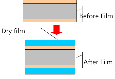
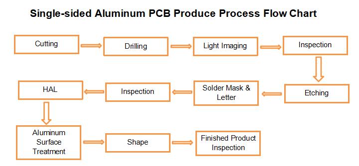
Single-sided copper clad laminate –> blanking –> (brushing, drying) –> drilling or punching –> screen printing circuit anti-etching graphics or use dry film –> curing inspection repair board –> etching copper –> Resist printing material removal, drying –> Brushing, drying –> Screen printing impedance pattern (commonly used green oil), UV curing –> Screen printing character mark pattern, UV curing –> Preheating, punching And appearance –> electrical open, short circuit test –> brushing, drying –> pre-coated soldering anti-oxidant (dry) or tin spraying hot air leveling –> inspection and packaging –> finished products leave the factory
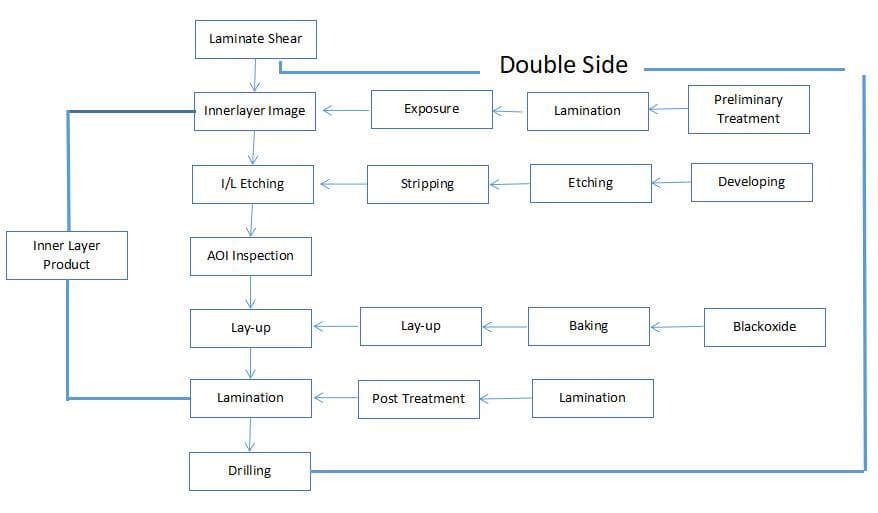
Double-sided Printed Circuit Board Manufacturing Process
Double-sided copper clad laminate –> blanking –> laminate –> CNC drilling via hole –> inspection, deburring and scrubbing –> electroless plating (via hole metallization) –> (full plate plating thin Copper) –> inspection brushing –> screen printing negative circuit graphics, curing (dry film or wet film, exposure, development) –> inspection, board repair –> circuit pattern electroplating –> electroplating tin (anti-corrosion Nickel/gold) –> Removing printing material (photosensitive film) –> Etching copper –> (Sn stripping) –> Cleaning and brushing –> Heat-curing green oil is commonly used for screen printing solder mask graphics (photosensitive wet film or Dry film, exposure, development, heat curing, commonly used photosensitive heat curing green oil) –> cleaning, drying –> screen printing character mark graphics, curing –> (tin or organic solder protection film) –> shape processing –> Cleaning and drying –> Electrical continuity detection –> Inspection and packaging –> Finished products leave the factory
Multi-layer Printed Circuit Board Manufacturing Process
Through-hole metallization process for manufacturing multilayer boards –> double-sided cutting of inner layer copper clad laminates –> brushing –> drilling positioning holes –> pasting photoresist dry film or coating photoresist –> Exposure –> Development –> Etching and film removal –> Inner layer roughening, deoxidation –> Inner layer inspection –> (Outer single-sided copper clad laminate circuit production, B-stage bonding sheet , plate bonding sheet inspection, drilling positioning hole) –> lamination –> numerical control drilling –> hole inspection –> hole pretreatment and electroless copper plating –> thin copper plating on the whole board –> coating Inspection –> pasting photoresistance electroplating dry film or coating photoresistance electroplating agent –> surface layer bottom plate exposure –> developing, repairing board –> circuit pattern electroplating –> electroplating tin-lead alloy or nickel / warp Plating –> Stripping and Etching –> Inspection –> Screen Printing Solder Mask Graphics or Photo Solder Mask Graphics –> Printing Character Graphics –> (Hot Air Leveling or Organic Soldering Film) –> CNC Wash shape –> Cleaning and drying –> Electrical continuity test –> Inspection and packaging –> Finished product leaving the factory

