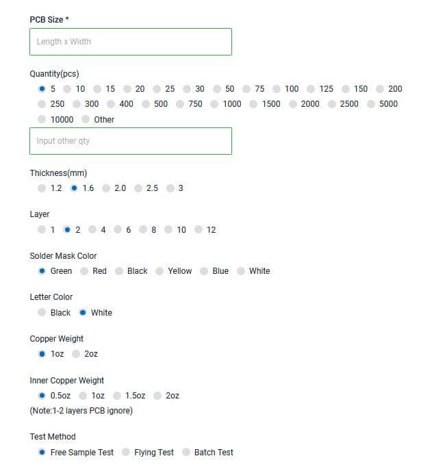
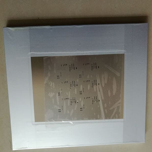
Printed circuit board (PCB) manufacturing involves several steps to create a functional PCB that can be used in electronic devices. Below is an overview of the typical PCB manufacturing process:
Design and Layout
The process begins with the design of the PCB. Engineers and designers use PCB design software to create a schematic diagram and layout of the circuit. This includes defining the placement and routing of components and traces.
Gerber Files
Once the PCB design is complete, Gerber files are generated. These files contain the information needed to manufacture the PCB, including layer information, component placement, and trace details.
Materials Selection
The choice of materials for the PCB is crucial. The most common material is a laminate consisting of layers of fiberglass or composite materials with copper foil bonded to them. The thickness and type of laminate are selected based on the specific requirements of the circuit.
Lamination
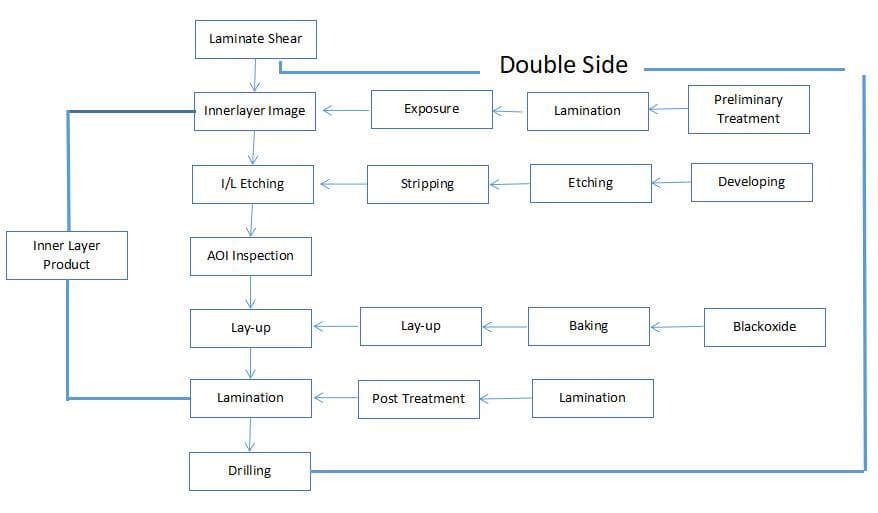
Multiple laminate layers are stacked, and the copper layers are aligned to create a single, multilayered board. The layers are bonded under heat and pressure to form a solid PCB.
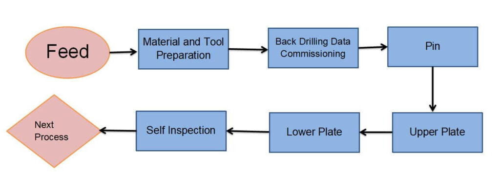
Drilling
Holes are drilled through the PCB at specific locations where components will be mounted. These holes may be through-hole vias or surface-mount pads for components.
Through-Hole Plating
To create electrical connections between different layers, the drilled holes are plated with a conductive material, typically copper. This process is known as electroplating.
Copper Etching
Unwanted copper is removed by etching the excess copper away from the surface, leaving only the desired traces and pads.
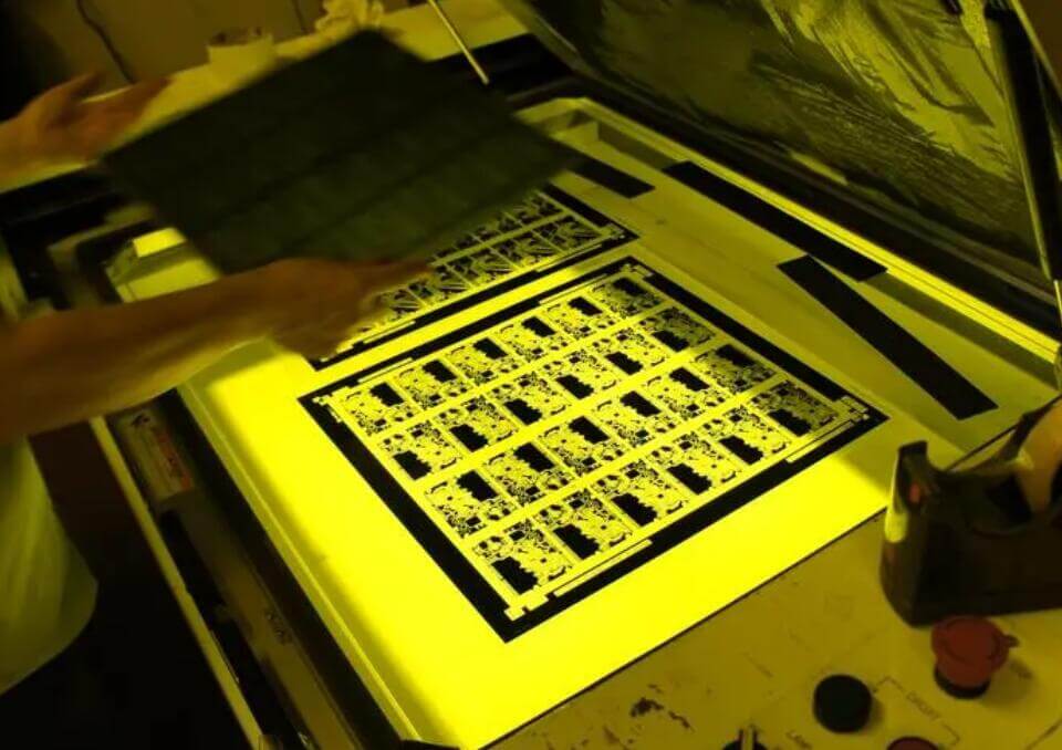
Silkscreen Printing
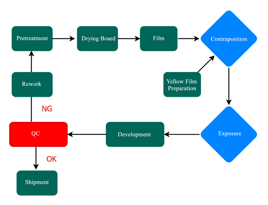
Information like component labels, reference designators, and other markings are printed on the PCB using a silkscreen process.
Solder Mask Application
A solder mask covers the entire board, leaving only the areas where components will be soldered exposed. This mask protects the board and ensures that solder only adheres to specific areas during assembly.
Surface Finish
The exposed copper surfaces are coated with a surface finish to improve solderability, prevent oxidation, and protect the copper traces. Common surface finishes include lead-free HASL, ENIG (Electroless Nickel Immersion Gold), and OSP (Organic Solderability Preservatives).
Component Assembly
Surface-mount components are placed on the PCB using automated pick-and-place machines. Through-hole components are inserted into their corresponding holes.
Soldering
Components are soldered onto the PCB using reflow soldering (for surface-mount components) or wave soldering (for through-hole components).
Testing
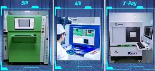
The assembled PCBs undergo various tests, including electrical testing, visual inspection, and functional testing, to ensure they meet quality and functionality standards.
Final Inspection
The final PCBs are inspected for defects, and quality control checks are performed.
Packaging and Shipping
Once the PCBs pass inspection, they are packaged and prepared for shipping to customers or assembly facilities.
The specific details and variations of the PCB manufacturing process can vary based on the complexity of the PCB design and the manufacturer’s capabilities. Additionally, some PCBs may require additional processes, such as applying conformal coatings for protection or special treatments for high-frequency applications.

