The Complete Guide to Multilayer PCBs
A Multilayer PCB is a circuit board containing three or more conductive material layers. These boards increase the available area for wiring. Whenever we talk about Multilayer, we consider some conductive patterns on the board. Multilayer PCB is usually rigid board because it is challenging to create it in a flexible format.
The number of layers depends on your needs. So the layers can be up to 100. However, 4 to 8 layers PCBs are commonly used in various applications. The circuit becomes complicated when the number of layers increases. So you can customize it according to your own needs and different layers.
Different Basic Components of Multilayer PCB
The main components of a multilayer PCB are as follows:
1. Substrate
It is the most important part, usually made of glass fiber. Glass fiber provides core strength to the PCB and prevents breakage. You can think of the substrate as the skeleton of the PCB.
2. Copper layer
It depends on the board type. So this layer can be full copper or copper foil. Regardless of the board type, the copper layer is still the same. Therefore, the copper carries the electrical signals in and out of the PCB.
3. Solder mask
It is a layer of polymer that protects the copper layer. So it prevents the short circuit when the copper is in contact with the environment. So you can think of the solder mask as the skin of the PCB.
4. Silkscreen
It is the last part of the PCB. The silkscreen shows the part number, symbol, and logo of the different components on the board. In addition, it also provides information such as symbol switch settings, test points, and component references.

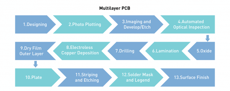
How to make a Multilayer PCB?
Here is a complete step-by-step guide for making a Multilayer PCB
1. Designing
The first and most crucial step is designing a PCB and preparing it for production. All manufacturers have their way of handling this process. Generally, the designer draws up the blueprint for the circuit and meets all outlined requirements. Different types of Software are available for design, such as Extended Gerber.
So you can use Extended Gerber or any other tool to design your circuit. Once you have designed the circuit, check the whole design carefully. Make sure the whole blueprint is error-free. After designing, you can send this blueprint to the fab to build the circuit.
2. Photo Drawing
You can use a laser plotter to draw the film for each layer at this step. A laser plotter is used to make photo tools for solder masks and silkscreen. The thickness of the film is about 7 mm.
Many manufacturers use special laser direct imaging equipment to image directly on the dry film. This technique reduces costs. In addition, the process is more accurate and efficient. Therefore, you can use direct laser imaging to generate inner and outer layers (LSI).
3. Imaging and Developing or Etching
This process applies the main images, such as pads and traces, to the board. Among other things, the DES process creates the copper pattern for plating. Here’s what this step does:
- Apply an imageable photo to a copper plate.
- Additionally, the panel is imaged using LSI.
- Etch away the entire exposed copper from the panel.
- Peel off the remaining dry film, leaving only the remaining copper pattern as the inner layer.
4. Automatic Optical Inspection
AOI inspects the different layers of a Multilayer PCB before all the layers are laminated together. Optics compares the PCB design data with the actual image on the panel. Any discrepancies, such as missing or extra copper, can result in an open or short circuit. This process helps the manufacturer find any defects in the circuit.
5. Oxide
Oxide is a chemical treatment of the inner layers before multilayer PCB lamination. Also, the oxidation code is brown or black, depending on the process. Increasing the roughness of the copper to enhance the bond strength of the laminate is a critical step. In addition, this process Prevents separation between different layers of the substrate.
6. Lamination
Different layers of epoxy resin-infused fiberglass are laminated to produce a Multilayer PCB. For lamination, manufacturers use hydraulic presses to apply high temperatures and pressure. The press and heat melt the fiberglass sheets and tightly bond the layers together. After cooling, this material follows the same manufacturing process as a double-sided PCB.
7. Drilling
All PCBs need holes to connect copper layers, connect components and mount the PCB. So you can drill holes using some advanced drilling systems. These systems use solid carbide cutters. Also, these are designed for quick removal of abrasive materials of debris.
A pre-programmed drilling machine drills a specific size hole at a precise location. So the drilling machine works according to the data provided by the designer. The designer offers this information as a CNC drilling file.
Besides, a thin aluminum sheet is used as an inlet material. Besides, cardboard is used as an outlet material. So this technique can keep drilling smoothly and avoid producing different fibers.
8. Electroless Copper Plating
After drilling the holes, manufacturers chemically deposit a thin layer of copper on the exposed surface of the panel. In addition, they use electroless plating to deposit a copper coating on the walls of the holes.
9. Dry Film Outer Layer
After the copper is deposited, you must apply the outer layer image to prepare the panel for plating. So you use a laminator to apply a dry film on the outer layer. Dry film is a photo-imageable material. Also, the process is almost similar to the Inner layers of multilayer PCBs that are imaged.
10. Plate
The electroplating process includes copper plating on the conductive pattern. Plus on the hole walls of the PCB. The thickness of the plating layer is about 1 thousand. After copper plating, you need to plate a thin layer of tin. The tin plating layer is used as an etch stop layer .
11. Stripes and Etches
After the plating process is done on the panel, the dry film remains. But you need to remove the underlying copper. Now the panel will go through the SES process. So SES stands for String Etch Strip.
During this process, you will need to etch the exposed copper. This means that you will remove the uncovered copper areas with tin. So the traces and pads around the holes and copper patterns remain there. Finally, you will chemically Remove the remaining tin covering the holes and traces. So after completing this step, you are left with only the laminate and copper of the exposed PCB.
At this stage, the skeleton of the PCB is now complete. All subsequent steps are now related to securing the PCB.
12. Solder Mask and Legend
Most manufacturers use an imageable liquid photo (LPI) solder mask to protect the copper surface. It further protects the solder bridges between different components during assembly.
LPI solder mask is basically a photosensitive epoxy-based resist. You can use a screen printing process to cover the entire panel. There are some other alternatives to traditional silkscreen plating. So you can use such options for solder masks.
After the solder mask, you can apply the legend. It prints different symbols and letters on the PCB for reference while assembling.
13. Surface Treatment
Surface treatment is the last and final chemical process in the manufacture of multilayer printed circuit boards. The solder mask covers nearly all of the circuitry. So the surface finish prevents oxidation of the remaining exposed copper areas.
Surface treatment is an essential step because you cannot solder copper oxide. Also, you can use different types of surface treatments in this step. For example, you can hot air solder horizontally (spray gun).
Benefits of Multilayer PCBs
Here are some advantages of multilayer PCBs over other types:
- It has higher assembly density than single-layer and double-layer PCBs.
- No cables are needed to interconnect different components. So it is ideal for low-weight PCB.
- These PCBs are smaller in size, reducing space requirements.
- EMI shielding is simple and flexible.
- Flexibility is another factor that makes multilayer PCBs stand out among all printed circuit boards.
How to identify Multilayer PCB?
You can follow these steps if you have some PCBs and want to check the total layers.
Exposing the board’s edge to light allows the copper planes to be seen. So in this way, you can easily observe the trance more closely. Even if the multilayer PCB does not contain blind vias, you can still use the bright light to analyze the internal Floor.
The best place to inspect the inner layers is where the paths and lines are not visible on the outer layers. Also, most manufacturers print labels to identify the total number of layers on the board. So just looking at the edges, you can determine the total number of layers.


